Graphene-based complementary type asymmetric n-type structure THz modulator and manufacture method therefor

A graphene-based, complementary technology, applied in the direction of instruments, nonlinear optics, optics, etc., can solve the problems of the decline of the quality factor of the Fano resonance line, the decrease of the Fano resonance amplitude, and the modulation effect is not very obvious, etc., to achieve the quality factor High, large modulation depth, effects with large modulation depth

Active Publication Date: 2018-09-14
SHANGHAI NORMAL UNIVERSITY
View PDF6 Cites 11 Cited by
  • Summary
  • Abstract
  • Description
  • Claims
  • Application Information

AI Technical Summary

Problems solved by technology

However, due to the strong photon energy in the mid-infrared band, the interband transition in graphene also plays a relatively large role, so the modulation effect is not very obvious
Li et al. studied the effect of the asymmetric parameters of the metal microstructure and the conductivity of graphene on the Fano resonance line by covering a whole piece of graphene on the asymmetric metal split ring. The results showed that the asymmetric Fano resonance line varies with With the increase of the asymmetry of the metal microstructure, the graphene has a significant modulation effect on the generated Fano resonance peak, resulting in a decrease in the Fano resonance amplitude and a decrease in the quality factor.
In this research work, the dynamic modulation of the Fano resonance peak cannot be achieved by changing the Fermi level, and the introduction of graphene leads to a significant decrease in the quality factor of the Fano resonance line, and the Q value is less than 3

Method used


Image

  • Graphene-based complementary type asymmetric n-type structure THz modulator and manufacture method therefor
  • Graphene-based complementary type asymmetric n-type structure THz modulator and manufacture method therefor
  • Graphene-based complementary type asymmetric n-type structure THz modulator and manufacture method therefor

Examples


Embodiment 1

[0059] The high-quality factor THz modulator of graphene complementary asymmetric Π-type microstructure, its preparation process is made through the following steps:

[0060] (1) Fabrication of polymer flexible substrate layer: ordinary Si sheet is used as a sacrificial layer, and the solution containing plastic polymer flexible substrate layer is sprayed on it by spincoating method, and then dried in an oven for about 30 minutes , the temperature range is 150-200 ° C, and then use a high-temperature furnace in an inert gas (or N 2 ) to 300-400°C (preferably 350°C) in a protective atmosphere to form a thin layer of uniform polymer flexible substrate layer;

[0061] (2) Making an epitaxial layer doped with Si: Form a semiconductor Si epitaxial layer 02 with a thickness of 1-10 μm by epitaxial growth method, and the doping concentration is 3×10 16 cm -3 , the electrical conductivity of the Si layer is 1-10Ω·cm, and the insulation is good, so as to reduce the loss;

[0062] (3...

Embodiment 2

[0071] The preparation method of the THz modulator based on graphene complementary type asymmetric Π type microstructure comprises the following steps:

[0072] (1) Making polymer flexible substrate layer

[0073] Using ordinary Si as a sacrificial layer, spray a solution containing a plastic flexible substrate on the sacrificial layer, dry it at 180°C for 20 minutes, and then heat it to 400°C under the protection of an inert gas for curing to obtain a polymer with a thickness of 1 μm. Flexible substrate layer;

[0074] (2) Fabrication of semiconductor epitaxial layer

[0075] Make the epitaxial layer doped with Si: form a doped Si layer with a thickness of 1 μm by epitaxial growth method, and the doping concentration is 10 15 cm -3 , the conductivity of the Si layer is 1Ω·cm;

[0076] (3) Make semiconductor ITO back electrode: make a semiconductor ITO thin layer as the back electrode by sputtering, with a thickness of about 20nm;

[0077] (4) Making Al 2 o 3 Insulation...

Embodiment 3

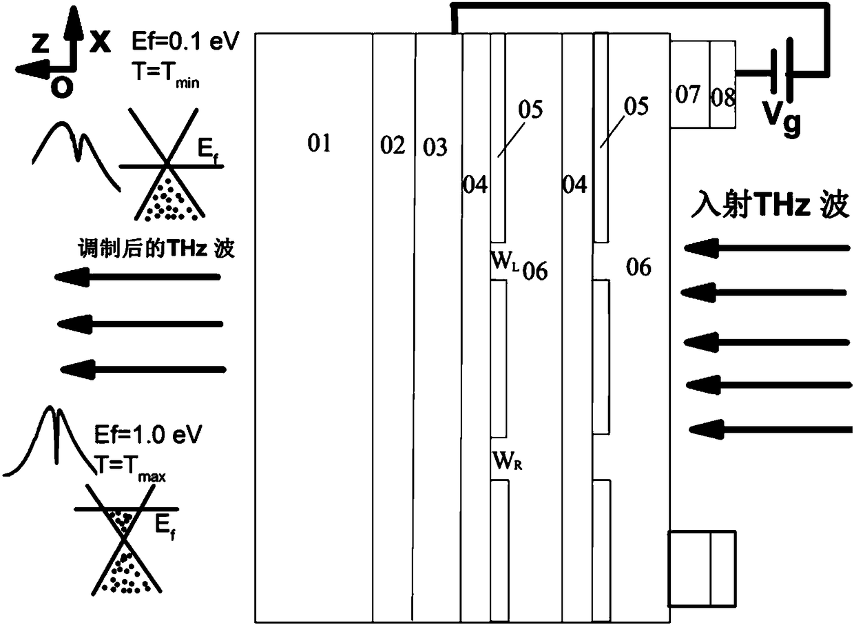
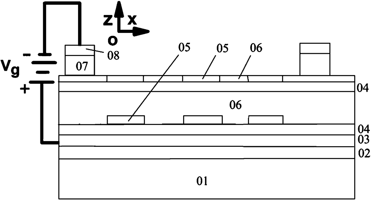
[0095] A graphene-based complementary asymmetric Π-structure THz modulator, comprising:

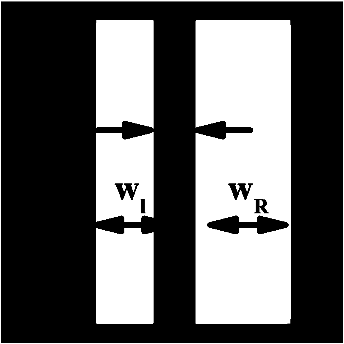
[0096] Polymer flexible substrate layer; semiconductor Si epitaxial layer: a doped semiconductor epitaxial layer formed by epitaxial growth method, with good insulation to achieve the purpose of reducing loss; semiconductor indium tin oxide sputtering layer, that is, the upper electrode semiconductor ITO (Indium Tin Oxide, Sn-doped indium oxide, an n-type semiconductor material with high conductivity) sputtering layer: sputtered on the semiconductor Si epitaxial layer, as the upper electrode of the THz modulator, the thickness is about 20nm; Al 2 o3 Insulation-active region structure composite layer: grown on the semiconductor indium tin oxide sputtering layer, made of at least one Al 2 o 3 Insulation-active region substructure stack composition, the Al 2 o 3 The insulating-active-region substructure includes the underlying Al 2 o 3 insulating layer, and grown on Al 2 o 3 Complemen...


PUM

PropertyMeasurementUnit
thicknessaaaaaaaaaa
thicknessaaaaaaaaaa
thicknessaaaaaaaaaa

Abstract

The invention relates to a graphene-based complementary type asymmetric n-type structure THz modulator and a manufacture method therefor. The THz modulator comprises a polymer flexible substrate layer, an indium tin oxide (ITO) semiconductor sputtering layer and an Al2o3 insulation-graphene active region structure composite layer, wherein the Al2o3 insulation-graphene active region structure composite layer is grown on an ITO layer and is formed by superposing at least one Al2o3 insulation-active region substructure, the Al2o3 insulation-active region substructure comprises an Al2o3 insulationlayer positioned on a lower part and a complementary type graphene microstructure layer grown on the Al2o3 insulation layer, and an electric conduction gel-gel layer is made as an upper electrode positioned on an uppermost active region substructure. Compared with technologies of the prior art, the modulator and the method disclosed in the invention are advantageous in that terahertz waves can beeffectively adjusted; the modulator are high in quality factors (Q)30), great in adjustable performance, and large in modulation depth and the like.

Description

technical field [0001] The invention relates to the technical field of semiconductor optoelectronic materials and devices, in particular to a high-quality factor THz modulator based on a graphene complementary asymmetric Π-type microstructure and a preparation method thereof. Background technique [0002] Terahertz (THz) waves lie between microwave and infrared radiation in the electromagnetic spectrum, in the transition region from electronics to photonics, and have broad prospects in both basic research and practical applications. As a key component of waveguide technology, modulator is of great value and significance to promote the development of THz technology in object imaging, biological sample analysis and short-range wireless communication. The current THz wave modulators can be divided into electro-modulation, photo-induced modulation and mechanical reconstruction modulation according to the modulation method, in which the electro-modulation realizes the control of ...

Claims


Application Information

Patent Timeline
Patent Type & Authority Applications(China)
IPC IPC(8): H01Q15/00G02F1/015
CPCG02F1/015H01Q15/0086
Inventor 何晓勇刘锋林方婷张浩
Owner SHANGHAI NORMAL UNIVERSITY
Why Eureka
Try Eureka