Supercharge Your Innovation With Domain-Expert AI Agents!

Copper-graphene composite coating on surface of integrated circuit ceramic circuit board and preparation method thereof

A ceramic circuit board and graphene composite technology, applied in the direction of coating, metal material coating process, superimposed layer plating, etc., can solve problems such as electroplating copper pollution, achieve good adhesion, reduce substrate temperature, and diffusion capacity. strong effect

Inactive Publication Date: 2019-12-24
WUHAN UNIV
View PDF5 Cites 1 Cited by
  • Summary
  • Abstract
  • Description
  • Claims
  • Application Information

AI Technical Summary

Problems solved by technology

In order to overcome the pollution problem of electroplating copper, the present invention combines arc ion plating, intermediate frequency magnetron sputtering, cold spray and vacuum heat treatment to develop a green and environmentally friendly copper plating technology on the surface of ceramic circuit boards.

Method used


Image

  • Copper-graphene composite coating on surface of integrated circuit ceramic circuit board and preparation method thereof
  • Copper-graphene composite coating on surface of integrated circuit ceramic circuit board and preparation method thereof
  • Copper-graphene composite coating on surface of integrated circuit ceramic circuit board and preparation method thereof

Examples


Embodiment 1

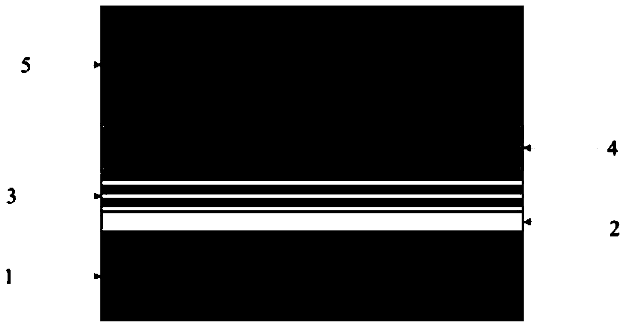
[0037] (1) In a vacuum environment, the surface of the ceramic circuit board is first cleaned with an arc ion source, and then the ceramic circuit board is ion-bombarded with high-pulse arc ion plating technology. The bombardment bias is 500V, and the high temperature of the plasma is used to form a metal diffusion layer. Layer depth 1 nm;

[0038] (2) On the basis of the diffusion layer, reduce the coating bias to prepare the metal bonding layer, and the deposition bias is 50V. The thickness of the bonding layer is 5 nanometers, and the grain size is 20 nanometers;

[0039] (3) After the preparation of the bonding layer is completed, open the intermediate frequency magnetron copper target, prepare Ti / Cu alternating multi-layer transition layer, Ti / Cu alternate multi-layer transition layer, the modulation cycle thickness is 10 nanometers, and the thickness of the single-layer Ti layer is 5 nanometers, the single-layer Cu thickness is 5 nanometers; the main purpose of the alte...

Embodiment 2

[0043] (1) In a vacuum environment, the surface of the ceramic circuit board is first cleaned with an arc ion source, and then the ceramic circuit board is ion-bombarded with a high-pulse arc ion plating technology. The bombardment bias is 1000V, and the high temperature of the plasma is used to form a metal diffusion layer. Layer depth 5 nm;

[0044] (2) On the basis of the diffusion layer, reduce the coating bias to prepare the metal bonding layer, and the deposition bias is 200V. The thickness of the bonding layer is 300 nanometers, and the grain size is 3 nanometers;

[0045] (3) After the preparation of the bonding layer is completed, open the intermediate frequency magnetron copper target, prepare Cr / Cu alternating multi-layer transition layer, Cr / Cu alternate multi-layer transition layer, the modulation cycle thickness is 100 nanometers, and the single-layer Cr layer thickness is 50 nanometers, the single-layer Cu thickness is 50 nanometers; the main purpose of the alt...

Embodiment 3

[0049] (1) In a vacuum environment, the surface of the ceramic circuit board is first cleaned with an arc ion source, and then the ceramic circuit board is bombarded with ions using high-pulse arc ion plating technology. Layer depth 5 nm;

[0050] (2) On the basis of the diffusion layer, reduce the coating bias to prepare the metal bonding layer, and the deposition bias is 150V. The thickness of the bonding layer is 200 nanometers, and the grain size is 20 nanometers;

[0051] (3) After the preparation of the bonding layer is completed, open the intermediate frequency magnetron copper target, prepare Zr / Cu alternating multi-layer transition layer, Zr / Cu alternate multi-layer transition layer, the modulation cycle thickness is 80 nanometers, and the thickness of the single-layer Zr layer is 40 nanometers, the single-layer Cu thickness is 40 nanometers; the main purpose of the alternating transition layer is to improve the bonding force between the Zr layer and the Cu layer, an...


PUM

PropertyMeasurementUnit
thicknessaaaaaaaaaa
thicknessaaaaaaaaaa
thicknessaaaaaaaaaa

Abstract

The invention discloses a copper and graphene composite coating on the surface of an integrated circuit ceramic circuit board and a preparation method of the copper and graphene composite coating. Thecomposite coating is composed of a transition metal (M) diffusion layer, a transition metal bonding layer, M / Cu alternating multilayer transition layer, an intermediate frequency magnetic control Cuthickening supporting layer and a cold spraying thickening Cu layer from inside to outside. In order to solve the pollution problem of electroplating copper, electric arc ion plating, medium-frequencymagnetron sputtering, cold spraying, vacuum heat treatment and other technologies are used in a combined mode in the preparation method of the composite coating. According to the copper and graphenecomposite coating on the surface of the integrated circuit ceramic circuit board and the preparation method of the copper and graphene composite coating, the multi-layer composite coating technology is fully utilized, so that the formed structure and composition are gradually changed, the coating and a substrate are in metallurgical bonding, and good adhesive force is achieved; compared with a conventional heat diffusion method, the preparation method has the advantages that the substrate temperature can be greatly reduced by adopting a coating technology, but a better copper coating can be obtained; the high-heat-conductivity and high-electricity-conductivity characteristics of graphene are utilized, so that the performance of a conventional copper coating is greatly improved; and a remarkable and environment-friendly ceramic circuit board surface copper plating technology is developed, and the industrial application prospect is good.

Description

technical field [0001] The invention belongs to the technical field of surface treatment, in particular to a copper-graphene composite coating on the surface of an integrated circuit ceramic circuit board and a preparation method thereof. Background technique [0002] With the gradual deepening of electronic technology in various application fields, highly integrated circuit boards have become an inevitable trend. Highly integrated packaging modules require a good heat dissipation carrying system, and the disadvantages of traditional circuit boards in terms of thermal conductivity have become restrictions on the development of electronic technology. a bottleneck. The ceramic substrate has excellent electrical insulation properties, excellent soldering characteristics, and high thermal conductivity. Its current-carrying capacity is very strong, and it can provide the most basic material for high-power electronic power circuit structure technology and interconnection technolo...

Claims


Application Information

Patent Timeline
Patent Type & Authority Patents(China)
IPC IPC(8): C23C14/16C23C14/18C23C14/32C23C14/35C23C14/58C23C24/04C23C28/02
CPCC23C14/165C23C14/18C23C14/325C23C14/35C23C14/5806C23C24/04C23C28/02
Inventor 杨兵李敬雨刘琰吴忠烨赵鑫
Owner WUHAN UNIV
Features
  • R&D
  • Intellectual Property
  • Life Sciences
  • Materials
  • Tech Scout
  • Unparalleled Data Quality
  • Higher Quality Content
  • 60% Fewer Hallucinations
Learn More