Preparation method of enhanced CMOS sensor light emitting diode unit structure

A CMOS sensor and light-emitting diode technology, applied in the direction of electrical components, semiconductor devices, circuits, etc., can solve the problem of unsuitable high-quality and uniform 2D imaging functions, the strict manufacturing of embedded chamfered Si structures, and large deviations in pixel characteristics etc. to achieve the effect of reducing edge scattering, reducing diffraction, and increasing signal-to-noise ratio

Active Publication Date: 2018-11-06
GUANGZHOU FENGSHANG ELECTRIC APPLIANCE
View PDF6 Cites 2 Cited by
  • Summary
  • Abstract
  • Description
  • Claims
  • Application Information

AI Technical Summary

Problems solved by technology

[0011] Random needle-like surface in c-Si with low reflectivity and high absorption efficiency; whereas CIS pixels with small pitch size contain random but limited number of structures, leading to large deviations in pixel characteristics, such as PRNU (photoresponse non-uniformity), Not suitable for high-quality uniform 2D imaging capabilities
[0012] The absolute critical angle of the embedded chamfered

Method used

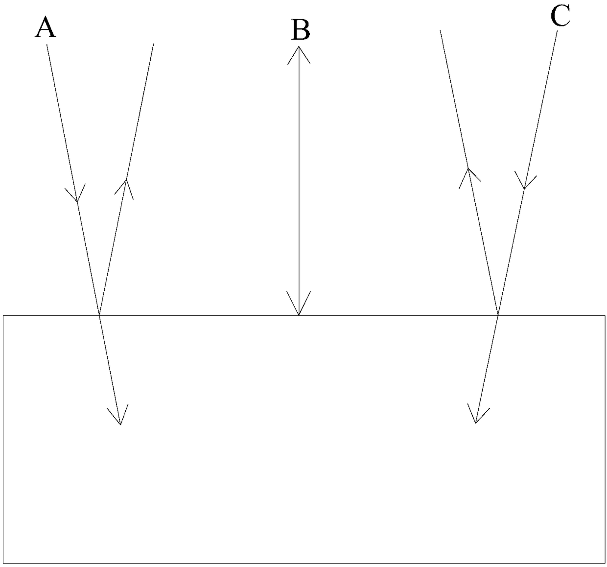
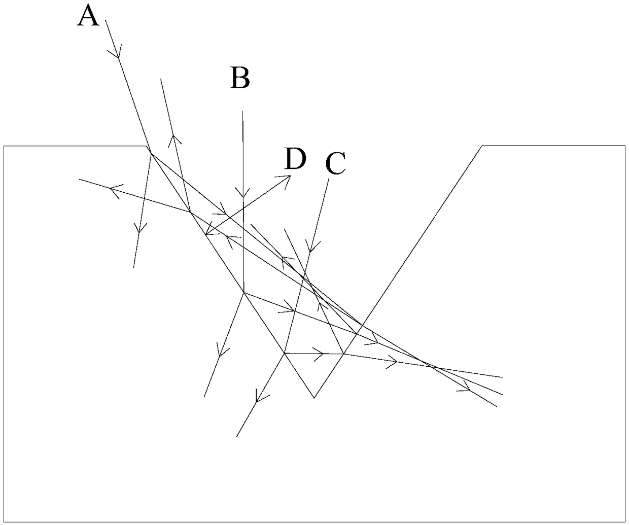
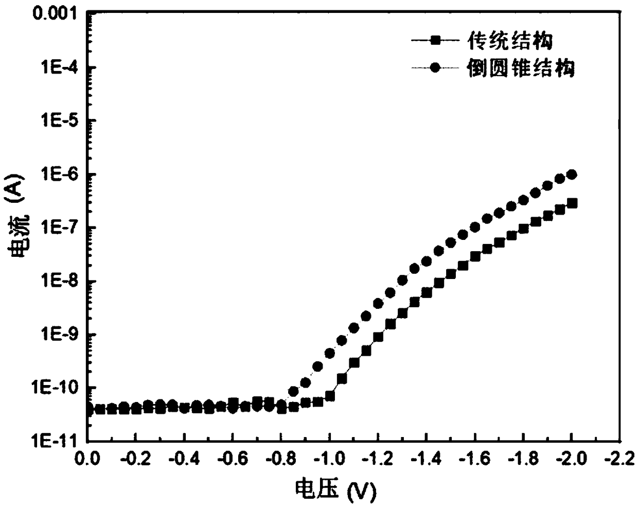

Image

  • Preparation method of enhanced CMOS sensor light emitting diode unit structure
  • Preparation method of enhanced CMOS sensor light emitting diode unit structure
  • Preparation method of enhanced CMOS sensor light emitting diode unit structure

Examples


Embodiment Construction

[0066] Embodiments of the present invention will now be described with reference to the drawings, in which like reference numerals represent like elements.

[0067] Please refer to Figure 2-19 , the preparation method of the enhanced CMOS sensor light-emitting diode unit structure, the steps include:

[0068] (1) Utilize the RCA cleaning method, rely on SC-1 cleaning solution, SC-2 cleaning solution, SC-3 cleaning solution, acid and deionized water to clean the P-type wafer 1, and peel off the P-type wafer 1 upper surface oxide layer. The P-type wafer material is silicon, and the thickness of the P-type wafer material is 700um. SC-1 cleaning solution is NH 4 OH / H 2 o 2 / H 2 O, SC-2 cleaning solution is HCI / H 2 o 2 / H 2 O, SC-3 cleaning solution is H 2 SO 4 / H 2 o 2 / H 2 O, the acid is HF. In the cleaning procedure, first remove the organic contamination on the surface of the silicon wafer, because organic matter will cover part of the surface of the silicon waf...


PUM

PropertyMeasurementUnit
Thicknessaaaaaaaaaa

Abstract

The invention discloses a preparation method of an enhanced CMOS sensor light emitting diode unit structure. The preparation method comprises the following steps: P-type wafer cleaning and surface oxide layer stripping, oxide layer coating, masking, configuring a square window for an oxide layer, high energy ion beam surface treatment, Si corrosion, masking and configuring the square window for the oxide layer, N-type doping, oxide layer coating, masking and oxide layer opening, P-type doing, oxide layer corrosion, silicide barrier layer coating, masking and opening, silicide coating, annealing, removeing unreacted silicide and barrier layer, nitrided layer coating, oxide layer coating, masking and configuring a lead contact hole, metal coating, chemical mechanical grinding, oxide layer coating, masking, oxide layer corrosion and wired metal coating. According to the preparation method of the enhanced CMOS sensor light emitting diode unit structure provided by the invention, the preparation process is simple, the quantum conversion efficiency can be enhanced, and the cost can be reduced.

Description

technical field [0001] The invention relates to the field of semiconductor manufacturing, in particular to the field of image sensors, in particular to a method for preparing an enhanced CMOS sensor light emitting diode unit structure. Background technique [0002] CMOS image chips convert charge into voltage at the pixel level, and most of the functions are integrated into the chip. This allows all functions to operate from a single power supply and enables flexible image readout according to regions of interest or windowing. [0003] CMOS image sensors are basically embedded with system-on-chip (SOC) structures such as analog-to-digital conversion (ADC), correlated double sampling (CDS), clock generation, and voltage regulators, or image post-processing, etc. Functions, which were previously only functions of application system-level design. The current CIS is usually produced according to the 1P5M process from 180nm to the recent 55nm, which allows the pixel design to a...

Claims


Application Information

Patent Timeline
IPC IPC(8): H01L33/00H01L33/20
CPCH01L33/0054H01L33/20
Inventor 楚双印李俊友谢涛刑美立
Owner GUANGZHOU FENGSHANG ELECTRIC APPLIANCE
Why Eureka
Try Eureka