

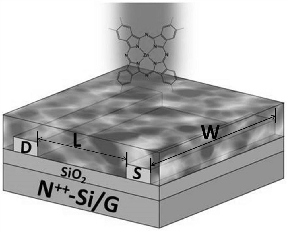
A kind of organic phototransistor and preparation method thereof
A phototransistor and organic technology, which is applied in the field of organic phototransistor and its preparation, can solve the problem of narrow spectral response range of the device, achieve excellent near-infrared spectrum absorption characteristics, improve stability, and reduce crystal defect density.
- Summary
- Abstract
- Description
- Claims
- Application Information
AI Technical Summary
Problems solved by technology
Method used
Image

Examples
preparation example Construction
[0044] The present invention also provides a method for preparing the above-mentioned organic phototransistor, comprising the following steps:
[0045] 1) Vacuum evaporation of gold electrodes on the insulating layer of the silicon base layer to obtain a silicon base plated with gold electrodes;
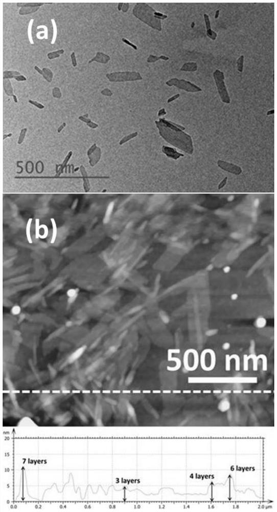
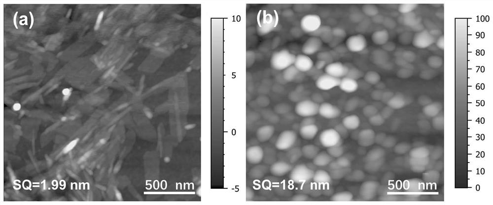
[0046] 2) Ultrasonic treatment of the metal zinc phthalocyanine formic acid dispersion was applied drop-coated on one side of the silicon substrate coated with gold electrodes to obtain a silicon substrate loaded with the dispersion;
[0047] 3) Annealing the silicon substrate loaded with the dispersion liquid to obtain an organic phototransistor.
[0048] In the invention, gold is used as a gold source, and a gold electrode is vacuum-evaporated on an insulating layer of a silicon base layer to obtain a silicon base plated with a gold electrode. In the present invention, the vacuum evaporation preferably includes sequentially cleaning and vacuum drying the silicon substrate.
[004...
Embodiment 1
[0069] 1) A silicon substrate (Si / SiO 2 ) into deionized water containing semiconductor cleaning agent, ultrasonically cleaned at room temperature for 10 min, taken out to dry; then placed in absolute ethanol, ultrasonically cleaned at room temperature for 10 min, taken out to dry; then placed in iso In propanol, ultrasonic cleaning at room temperature for 10 min, take out to dry; then place in acetone, ultrasonic cleaning at room temperature for 10 min, take out with N 2 Blow dry; finally put it into a vacuum drying oven, vacuum dry at 120° C. overnight, and set aside.
[0070] 2) The cleaned silicon substrate (Si / SiO 2 ) placed on the substrate stage of a vacuum evaporation apparatus (Mbraun MB200), and the vacuum degree of the control chamber is not lower than 5×10 -6 mbar, with high-purity gold (99.999%) as the gold source, gold electrodes were evaporated on the insulating layer of the silicon substrate at a rate of 0.3 Å / s, and the electrode thickness was controlled at...
Embodiment 2
[0097] 1) A silicon substrate (Si / SiO 2 ) into deionized water containing semiconductor cleaning agent, ultrasonically cleaned at room temperature for 10 min, taken out to dry; then placed in absolute ethanol, ultrasonically cleaned at room temperature for 10 min, taken out to dry; then placed in iso In propanol, ultrasonic cleaning at room temperature for 10 min, take out to dry; then place in acetone, ultrasonic cleaning at room temperature for 10 min, take out with N 2 Blow dry; finally put it into a vacuum drying oven, vacuum dry at 120° C. overnight, and set aside.
[0098] 2) The cleaned silicon substrate (Si / SiO 2 ) placed on the substrate stage of a vacuum evaporation apparatus (Mbraun MB200), and the vacuum degree of the control chamber is not lower than 5×10 -6 mbar, with high-purity gold (99.999%) as the gold source, gold electrodes were evaporated on the insulating layer of the silicon substrate at a rate of 0.3 Å / s, and the electrode thickness was controlled at...
PUM
| Property | Measurement | Unit |
|---|---|---|
| thickness | aaaaa | aaaaa |
| thickness | aaaaa | aaaaa |
| thickness | aaaaa | aaaaa |
Abstract
Description
Claims
Application Information