A method for preparing patterned ordered bimetallic nanoparticle array by annealing method

A bimetallic nano-patterning technology, which is applied in semiconductor/solid-state device manufacturing, electrical components, circuits, etc., can solve problems such as the inability to achieve high-density patterned nano-particle distribution, the inability to be widely used, and the inability to make the distance small. Achieve the effect of controllable pattern, high stability and controllable particle size

Active Publication Date: 2022-07-22
CHANGCHUN UNIV OF SCI & TECH
View PDF13 Cites 0 Cited by
  • Summary
  • Abstract
  • Description
  • Claims
  • Application Information

AI Technical Summary

Problems solved by technology

[0004] Existing processes for preparing patterned substrates with nanostructures, such as laser interference lithography, ion etching, and nanoimprinting, require multi-step etching processes and pattern transfer processes, and cannot be widely used due to the limitations of small preparation area and low production capacity. application
At the same time, the existing method of patterning the substrate to control the position of the generated metal nanoparticles relies on the morphology of the substrate. If each nanostructure is limited to one nanoparticle, the distance between the particles cannot be made small, that is, it cannot achieve high density. Patterned Nanoparticle Distribution

Method used


Image

  • A method for preparing patterned ordered bimetallic nanoparticle array by annealing method
  • A method for preparing patterned ordered bimetallic nanoparticle array by annealing method
  • A method for preparing patterned ordered bimetallic nanoparticle array by annealing method

Examples


Embodiment 1

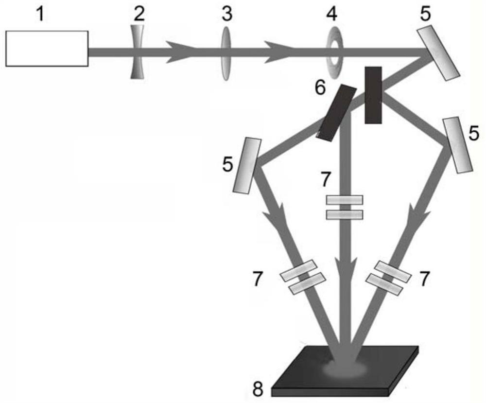
[0033] like figure 1 As shown, the present invention adopts the annealing method to prepare the method for periodically patterned bimetallic nanoparticles as follows:

[0034] (1) Prepare a patterned substrate by laser interference: build a laser interference system according to the expected pattern (5μm side length hexagonal array), select a 1064nm Nd:YAG nanosecond laser (pulse width is 6ns, repetition rate is 10Hz), and the light splits The system generates three coherent beams and adjusts the energy density of the interference laser to 400mJ / cm 2 , the interference light acts vertically on the surface of the single-sided polished (100) oriented single-crystal silicon wafer for 5 seconds, and ablates a hexagonal array pattern with a side length of 5 μm.

[0035] figure 2 It is a three-beam laser interference ablation system, including a 1064nm nanosecond laser 1, a concave lens 2, a convex lens 3, a variable aperture 4, a mirror 5, a beam splitter 6, a half-wave plate an...

Embodiment 2

[0042] In Example 2, the energy density of the interference laser was adjusted to 350mJ / cm 2 , other experimental parameters are consistent with Example 1, and the results are as follows Figure 7 shown.

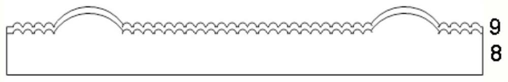
[0043] The silicon substrate after laser interference ablation was tested by scanning electron microscope SEM, and the results were as follows Figure 7 shown in a. Since the intensity of the interference laser has a periodic Gaussian distribution, when it acts on the surface of the silicon material, the silicon surface is ablated, melted, evaporated, and solidified with high energy, and has a nanostructure distribution. In this embodiment, the size of the nanostructure is about 10 nm. Under the action of low energy, the silicon surface did not reach the melting threshold and did not change, forming a microstructure pattern consistent with the laser interference pattern, with a micrometer scale of 5 μm. Microstructure patterns and nanostructures form periodic cross-scale ...

Embodiment 3

[0046] In Example 3, the energy density of the interference laser was adjusted to 500 mJ / cm 2 , other experimental parameters are consistent with Example 1, and the results are as follows Figure 8 shown.

[0047] The silicon substrate after laser interference ablation was tested by scanning electron microscope SEM, and the results were as follows Figure 8 shown in a. Since the intensity of the interference laser has a periodic Gaussian distribution, when it acts on the surface of the silicon material, the silicon surface is ablated, melted, evaporated, and solidified with a nanostructure distribution. In this embodiment, the nanostructure size is about 30 nm. Under the action of low energy, the silicon surface did not reach the melting threshold and did not change, forming a microstructure pattern consistent with the laser interference pattern, with a micrometer scale of 5 μm. Microstructure patterns and nanostructures form periodic cross-scale micro / nanostructure pattern...


PUM

PropertyMeasurementUnit
thicknessaaaaaaaaaa
wavelengthaaaaaaaaaa
thicknessaaaaaaaaaa

Abstract

The invention relates to a method for preparing a patterned ordered bimetal nanoparticle array by using an annealing method. By using a two-step processing method of laser interference ablation and metal thin film annealing, firstly, laser interference is used to ablate a periodic cross-scale on a silicon wafer. The micro / nanostructure pattern is formed, and a double-layer metal film with a specific thickness is sputtered on the silicon substrate. During the annealing process, the de-wetting property of the metal film on the surface of the patterned silicon substrate is used to realize the template of metal nanoparticles. Self-assembled, resulting in ordered bimetallic nanoparticle arrays consistent with laser interference patterns. The invention can obtain a large-area patterned and orderly bimetallic nanoparticle array, the preparation method is simple and does not require pattern transfer and chemical synthesis, and has the advantages of controllable particle size and composition, controllable pattern, good repeatability and high stability.

Description

technical field [0001] The invention relates to a preparation method of a patterned ordered bimetallic nanoparticle array, and belongs to the technical field of nanoparticle preparation. Background technique [0002] Compared with single metal nanoparticles, bimetallic nanoparticles composed of two different metal elements have more flexible compositions and structures, and exhibit some more special physical and chemical properties. In particular, patterned bimetallic nanoparticle arrays have potential applications in plasmonic devices, magnetic storage, surface Raman enhancement, and catalysis of carbon nanotube and nanowire growth. Bimetallic nanoparticles have attracted extensive attention in the scientific community. For example, gold (Au) nanomaterials have a wide range of applications in the field of catalysis, but are limited by reserves. Using Co, Ni and other magnetic metals combined with Au nanoparticles to prepare magnetic Au-based heterojunction nanocatalytic ma...

Claims


Application Information

Patent Timeline
Patent Type & Authority Patents(China)
IPC IPC(8): H01L21/203H01L21/302H01L21/3065
CPCH01L21/203H01L21/302H01L21/3065
Inventor 王作斌王璐于化东许金凯董莉彤李理翁占坤
Owner CHANGCHUN UNIV OF SCI & TECH
Why Eureka
Try Eureka