Perovskite light emitting diode based on ultraviolet thermal annealing process and a preparation method thereof

A light-emitting diode, perovskite technology, applied in semiconductor/solid-state device manufacturing, electrical components, electrical solid-state devices, etc., can solve the problems of poor stability, large leakage current, weak device brightness, etc., and achieve strong resistance to water and oxygen corrosion. , The effect of solving large performance deviation and improving brightness and efficiency

Active Publication Date: 2019-01-22
UNIV OF ELECTRONICS SCI & TECH OF CHINA
View PDF5 Cites 9 Cited by
  • Summary
  • Abstract
  • Description
  • Claims
  • Application Information

AI Technical Summary

Problems solved by technology

[0004] The purpose of the present invention is to solve the problems of poor film quality, many crystal defects and large leakage current, resulting in weak device brightness and low efficiency, and the perovskite film is resistant to water and oxygen corrosion. Th

Method used


Image

  • Perovskite light emitting diode based on ultraviolet thermal annealing process and a preparation method thereof
  • Perovskite light emitting diode based on ultraviolet thermal annealing process and a preparation method thereof

Examples


preparation example Construction

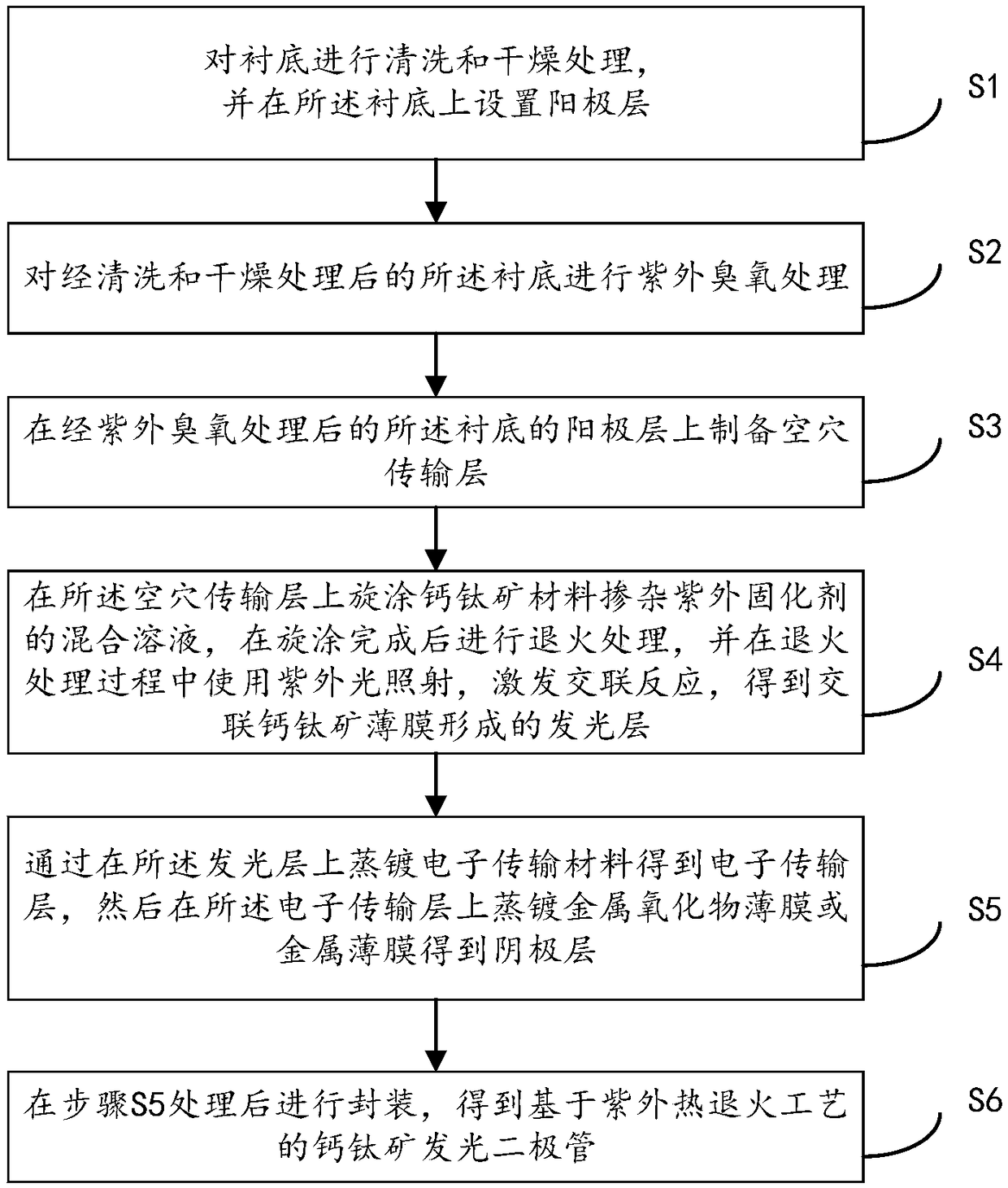
[0034] A preparation method of perovskite light emitting diode based on ultraviolet thermal annealing process, such as figure 1 Shown, including:

[0035] S1, cleaning and drying the substrate, and setting an anode layer on the substrate;

[0036] S2, performing ultraviolet ozone treatment on the substrate 10 after the cleaning and drying treatment;

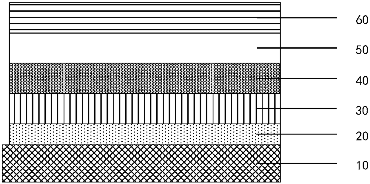
[0037] S3: preparing a hole transport layer 30 on the anode layer 20 of the substrate 10 after the ultraviolet ozone treatment;

[0038] S4. Spin-coating a mixed solution of perovskite material doped with ultraviolet curing agent on the hole transport layer 30, and perform annealing treatment after the spin coating is completed, and irradiate with ultraviolet light during the annealing treatment to stimulate the cross-linking reaction , To obtain a light-emitting layer 40 formed of a cross-linked perovskite film;

[0039] S5. Obtain an electron transport layer 50 by evaporating an electron transport material on the light-emitting layer 40...

Embodiment 1

[0053] This embodiment provides a method for manufacturing a perovskite light-emitting diode based on an ultraviolet thermal annealing process, including:

[0054] Step 1. Use transparent conductive substrate ITO glass as the substrate 10, ultrasonically clean the substrate 10 with ethanol solution, acetone solution, and deionized water, and then use dry nitrogen to blow dry, and remove the substrate 10 The upper ITO film is used as the anode layer 20 of the diode device; the resistance of the ITO film on the transparent conductive substrate ITO glass used is 10Ω / sq;

[0055] Step 2. Perform ultraviolet ozone treatment on the substrate 10 after cleaning and drying for 15 minutes;

[0056] Step 3. Spin-coating PEDOT:PSS on the anode layer 20 of the substrate 10 after the ultraviolet ozone treatment, and then perform annealing treatment to form a hole transport layer 30;

[0057] Step 4. Transfer to a nitrogen environment (such as a glove box with a 99.9% nitrogen atmosphere), and spin-...

Embodiment 2

[0061] This embodiment provides a method for manufacturing a perovskite light-emitting diode based on an ultraviolet thermal annealing process, including:

[0062] Step 1. Use the transparent conductive substrate ITO glass as the substrate 10, clean and dry the substrate 10, and use the ITO film on the substrate 10 as the anode layer 20 of the diode device; the transparent conductive The resistance of the ITO film on the substrate ITO glass is 10Ω / sq;

[0063] Step 2. Perform ultraviolet ozone treatment on the substrate 10 after cleaning and drying for 15 minutes;

[0064] Step 3. Spin-coating PEDOT:PSS on the anode layer 20 of the substrate 10 after the ultraviolet ozone treatment, and then perform annealing treatment to form a hole transport layer 30;

[0065] Step 4. Transfer to a nitrogen environment (such as a glove box with a 99.9% nitrogen atmosphere), and spin-coat MAPbBr on the hole transport layer 30 3 A mixed solution of 3,3',4,4'-benzophenone tetracarboxylic dianhydride do...


PUM

PropertyMeasurementUnit
Thicknessaaaaaaaaaa
Thicknessaaaaaaaaaa
Thicknessaaaaaaaaaa

Abstract

The invention discloses a perovskite light emitting diode based on an ultraviolet thermal annealing process and a preparation method thereof. The preparation method comprises the following steps: cleaning and drying the substrate, and arranging an anode layer on the substrate; And then carrying out ultraviolet ozone treatment; And then preparing a hole transport layer on the anode layer of the substrate; spin-coating The mixed solution of perovskite material doped with UV curing agent on the hole transport layer, then annealed and irradiated with UV light to obtain the cross-linked perovskitefilm luminescent layer. And preparing an electron transport layer and a cathode layer by vapor deposition on the light emitting layer; Finally performing encapsulation. perovskite material is doped with an ultraviolet curing agent and the ultraviolet light is irradiate to prepare a luminescent layer, the generated perovskite thin film is dense, continuous, good in crystallinity and strong in water-oxygen corrosion resistance, so that the brightness and efficiency of the perovskite light-emitting diode are improved, and the stability of the device is improved.

Description

Technical field [0001] The invention belongs to the technical field of electronic components, and particularly relates to a perovskite light-emitting diode based on an ultraviolet thermal annealing process and a preparation method. Background technique [0002] Organic-inorganic hybrid perovskite materials can be represented by the chemical formula MAPbX3, where X is Br, I, and Cl. This type of material has excellent characteristics such as high carrier mobility, high fluorescence quantum yield, adjustable bandwidth, etc. It can be widely used in photovoltaic devices such as solar cells, photodetectors and light-emitting diodes. Among them, light-emitting diodes based on perovskite materials have the characteristics of high luminous purity, high emission efficiency and low excitation energy, which have attracted widespread attention in the academic community. Since 2014, Professor Friend’s research group prepared perovskite light-emitting diodes at room temperature for the first ...

Claims


Application Information

Patent Timeline
IPC IPC(8): H01L51/50H01L51/56
CPCH10K71/12H10K71/421H10K50/12H10K71/00
Inventor 郭浩高瞻王子君于军胜
Owner UNIV OF ELECTRONICS SCI & TECH OF CHINA
Why Eureka
Try Eureka