A method for preparing a chain-type wet-process black silicon cell with high conversion efficiency

A high-conversion, solar cell technology, applied in the field of solar cells, to achieve the effect of improving conversion efficiency, low recombination rate, and reducing recombination rate

Active Publication Date: 2020-08-11
HENGDIAN GRP DMEGC MAGNETICS CO LTD
View PDF7 Cites 0 Cited by
  • Summary
  • Abstract
  • Description
  • Claims
  • Application Information

AI Technical Summary

Problems solved by technology

Therefore, the existing wet-process black silicon has been difficult to make a big breakthrough in battery conversion efficiency.

Method used


Image

  • A method for preparing a chain-type wet-process black silicon cell with high conversion efficiency
  • A method for preparing a chain-type wet-process black silicon cell with high conversion efficiency
  • A method for preparing a chain-type wet-process black silicon cell with high conversion efficiency

Examples


preparation example Construction

[0060] A method for preparing a high-conversion-efficiency chain-type wet-process black silicon solar cell, comprising the following steps:

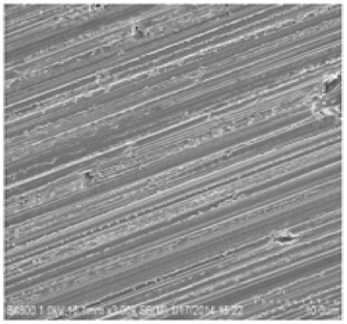
[0061] 1) Select P-type polycrystalline diamond wire silicon wafers, sequentially wash with organic alkali solution and water, and dry;

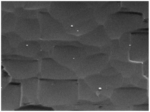
[0062] 2) Coating SiON:H film on the back and around the silicon wafer;

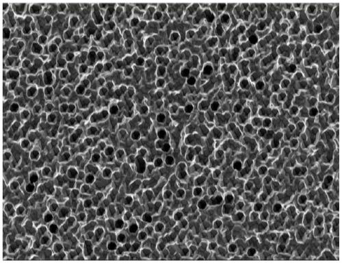
[0063] 3) Make a black silicon suede surface on the front side of the silicon wafer;

[0064] 4) Diffusion is performed on the front side of the silicon wafer to form a PN junction on the front side;

[0065] 5) Pickling with an acid solution to remove the phosphosilicate glass on the front of the silicon wafer and corroding the SiON:H film on the back and around the silicon wafer, then washing with water and drying;

[0066] 6) Anti-reflection film is coated on the black silicon suede surface, and no anti-reflection film is coated on the back of the silicon wafer;

[0067] 7) Print the positive electrode on the front side of ...

Embodiment 1

[0086] 1) Diamond wire polysilicon wafers use chain-type organic alkali cleaning equipment. The volume ratio of tetramethylammonium hydroxide to pure water is 1:15, and the cleaning time is 200s. cleaning process.

[0087] 2) The silicon wafer is inserted into the graphite boat carrier using tubular coating equipment. The back of the silicon wafer is coated with SiON:H film with a film thickness of 100nm and a refractive index of 1.85. Using silane flow rate of 500 sccm, ammonia gas flow rate of 5000 sccm, nitrous oxide gas flow rate of 7000 sccm and deposition pressure of 1500 mTorr, the total time for depositing SiON:H film on the back of the silicon wafer is 45 min.

[0088] 3) Silicon wafer coated with SiON:H film enters chain-type wet black silicon equipment. The front side of the silicon wafer is made of black silicon suede. Suede surface, but the SiON:H film on the back of the silicon wafer reacts with the hydrofluoric acid solution in the wet black silicon equipment, ...

Embodiment 2

[0098] 1) Diamond wire polysilicon wafers use chain-type organic alkali cleaning equipment. The volume ratio of tetramethylammonium hydroxide to pure water is 1:5. The cleaning time is 200s. cleaning process.

[0099] 2) The silicon wafer is inserted into the graphite boat carrier using tubular coating equipment, and the back of the silicon wafer is coated with SiON:H film with a film thickness of 150nm and a refractive index of 2.0. Using silane flow rate of 700 sccm, ammonia gas flow rate of 3000 sccm, nitrous oxide gas flow rate of 4000 sccm and deposition pressure of 1500 mTorr, the total time for depositing SiON:H film on the back of the silicon wafer is 50 min.

[0100] 3) Silicon wafers coated with SiON:H film enter chain-type wet black silicon equipment. The front side of the silicon wafer is made of black silicon suede. The size of the suede is 800nm, and the reflectivity is 19%. Suede surface, but the SiON:H film on the back of the silicon wafer reacts with the hydr...


PUM

PropertyMeasurementUnit
thicknessaaaaaaaaaa
reflectanceaaaaaaaaaa
particle diameteraaaaaaaaaa

Abstract

The invention relates to the field of solar cells and discloses a preparation method of a chain wet black silicon cell chip with high conversion efficiency, which comprises the following steps: 1) selecting P-type polycrystalline diamond wire silicon chip, cleaning and drying with organic alkali solution and water in turn; 2) plating a SiON: H film on that back surface and the periphery of the silicon wafer; 3) manufacturing a black silicon pile surface on that front surface of the silicon wafer; 4) diffusing that front surface of the silicon wafer to form a PN junction; 5) removing that phosphorus-silicon glass on the front side of the silicon wafer and etch the back side of the silicon wafer and the SiON: H films around the silicon wafer with an acid solution, washing with water and drying; 6) plating an antireflection film on that black silicon pile surface; 7) printing that positive electrode on the front side of the silicon wafer; 8) printing the back side of the silicon wafer andsintering. The conversion efficiency of the black silicon battery chip prepared by the method of the invention is effectively improve, and is suitable for the technical upgrading of the subsequent polycrystalline battery chip such as the black silicon + PERC series battery, the black silicon + MWT series battery and the like.

Description

technical field [0001] The invention relates to the field of solar cells, in particular to a method for preparing chain-type wet-process black silicon solar cells with high conversion efficiency. Background technique [0002] Solar photoelectric power generation is one of the clean, environmentally friendly and sustainable energy utilization forms, and it has developed rapidly in the world in recent years. At present, crystalline silicon solar cells are the mainstream field of photovoltaic power generation, but due to their high cost, they cannot replace traditional energy sources for the time being. Reducing costs and increasing photoelectric conversion efficiency have become the biggest problem in the photovoltaic industry. In the existing conventional production technology, polycrystalline diamond wire silicon wafers are made of micron-scale worm-like structures by acid texturing, and the reflectivity of polycrystalline silicon is about 24-30%. less efficient. Among the...

Claims


Application Information

Patent Timeline
Patent Type & Authority Patents(China)
IPC IPC(8): H01L31/18H01L31/0236H01L31/0224
CPCH01L31/022441H01L31/02366H01L31/1804H01L31/1868Y02E10/547Y02P70/50
Inventor 许成德陈健生李鑫
Owner HENGDIAN GRP DMEGC MAGNETICS CO LTD
Why Eureka
Try Eureka