High-thermal stability chip-scale LED (Light Emitting Diode) packaging method and product
A LED packaging and chip-level technology, applied in semiconductor devices, electrical components, circuits, etc., can solve problems such as difficulty in controlling the uniformity of the phosphor layer, affecting the repeatability of LED products, consistency of light and color, and poor thermal stability. Light color consistency and process integration, meet thermal stability requirements, and strong thermal reliability
- Summary
- Abstract
- Description
- Claims
- Application Information
AI Technical Summary
Problems solved by technology
Method used
Image

Examples
Embodiment 1
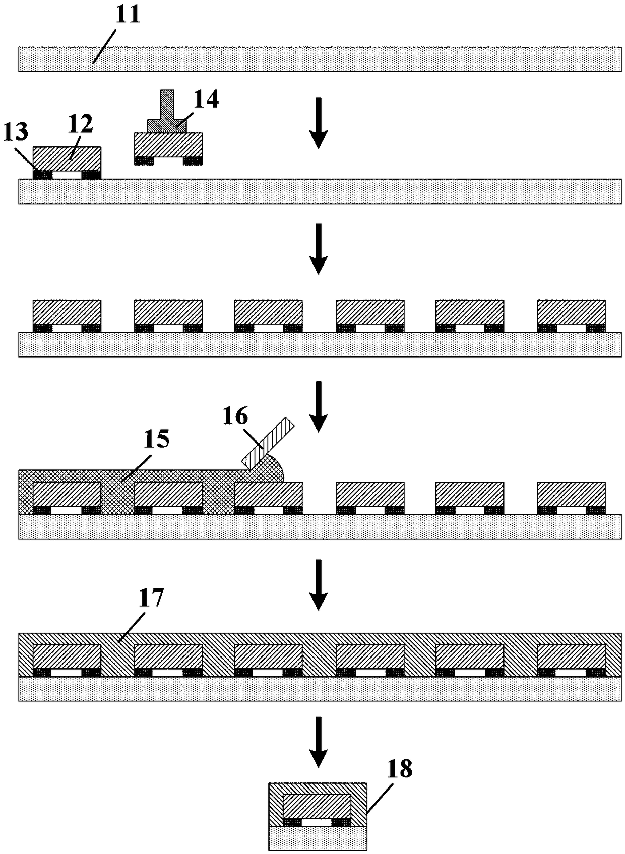
[0052] see figure 1 , the embodiment 1 provides a highly thermally stable chip-scale LED packaging structure, the LED chip 12, the ceramic substrate 11 and the fluorescent glass layer 17. The LED chip 12 is mounted on the circuit layer of the ceramic substrate 11 through eutectic bonding, and the electrical interconnection is realized through the solder joints 13. Preparation of sintered fluorescent glass paste 15 .
[0053] The chip-level LED packaging method of the present embodiment 1 may include the following steps as an example:
[0054] Step 1, the selected high-quality blue-ray flip-chip LED chips 12 are mounted on the circuit layer of the ceramic substrate 11 through the eutectic bonding head 14 of the eutectic bonding machine;
[0055] Step 2, coating the fluorescent glass paste 15 with a uniform thickness on the ceramic substrate 11, the paste layer covers the top and side of the LED chip 12, and the scraper 16 is controlled to adjust the thickness and uniformity o...
Embodiment 2
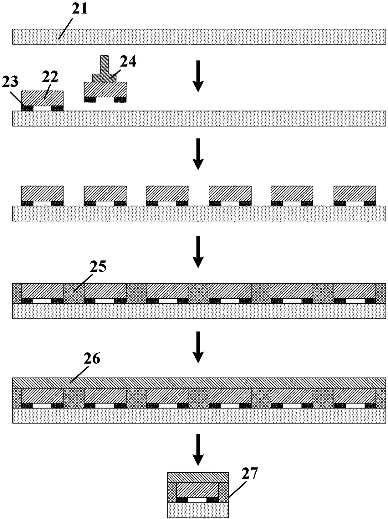
[0060] see figure 2 , this embodiment provides another chip-scale LED packaging structure with high thermal stability, including LED chips 22 , ceramic substrate 21 , light-shielding layer 25 and fluorescent glass sheet 26 . The LED chip 22 is eutectically bonded on the circuit layer of the ceramic substrate 21, and is electrically interconnected through solder joints 23. The light blocking layer 25 is coated on the side of the LED chip 22, and the fluorescent glass sheet 26 is bonded to the LED chip 22 top.
[0061] The manufacturing method of the present embodiment comprises the following steps:
[0062] Step 1, the selected high-quality ultraviolet flip-chip LED chip 22 is mounted on the circuit layer of the ceramic substrate 21 through the eutectic welding head 24 of the eutectic bonding machine;
[0063] Step 2, coating the light-blocking layer 25 between the LED chips 22, controlling its height to be the same as the thickness of the LED chip 22 by grinding the light-b...
PUM
| Property | Measurement | Unit |
|---|---|---|
| Glass transition temperature | aaaaa | aaaaa |
| Glass transition temperature | aaaaa | aaaaa |
| Temperature tolerance | aaaaa | aaaaa |
Abstract
Description
Claims
Application Information
 - R&D
- Intellectual Property
- Life Sciences
- Materials
- Tech Scout
- Unparalleled Data Quality
- Higher Quality Content
- 60% Fewer Hallucinations
Browse by: Latest US Patents, China's latest patents, Technical Efficacy Thesaurus, Application Domain, Technology Topic, Popular Technical Reports.
© 2025 PatSnap. All rights reserved.Legal|Privacy policy|Modern Slavery Act Transparency Statement|Sitemap|About US| Contact US: help@patsnap.com