Transparent conductive substrate and its preparation method and application
A technology of transparent conductive and transparent substrates, applied in cable/conductor manufacturing, conductive layers on insulating carriers, circuits, etc., can solve the problems of complex operation, low yield, inconsistent product quality, etc., and achieve high transparency and electrical conductivity. Consistent, transparent effects
- Summary
- Abstract
- Description
- Claims
- Application Information
AI Technical Summary
Problems solved by technology
Method used
Image

Examples
preparation example Construction
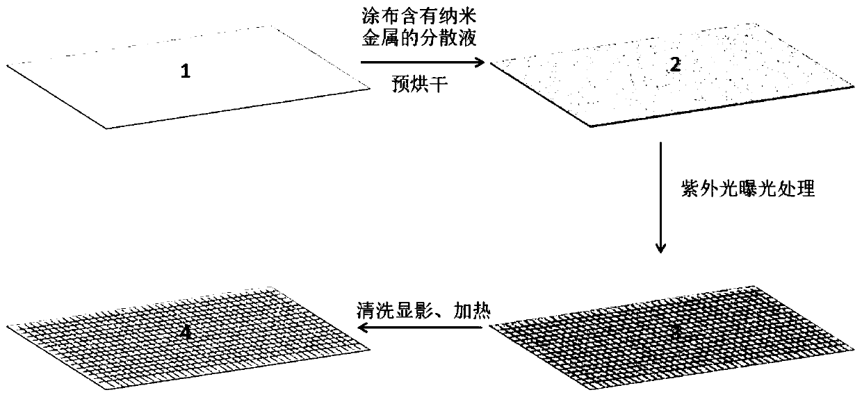
[0039] The first aspect of the present invention provides a method for preparing a transparent conductive substrate, such as figure 1 As shown, wherein, the method includes the following steps:
[0040] (A) uniformly coating the dispersion liquid containing the nano metal on the surface of the transparent substrate 1, and pre-drying to obtain the substrate 2 coated with the nano metal coating;
[0041] (B) Exposing the substrate 2 coated with the nano-metal coating to ultraviolet light to form a light-cured stereotyped conductive grid 3 containing the nano-metal with a grid line width ≤ 20 μm, and then cleaning, developing, and heating, A transparent conductive substrate 4 is obtained;
[0042] The nanometer metal is an ultraviolet light sensitive substance.
[0043] According to the method of the present invention, the grid line width refers to the characteristic width of the projected grid formed by ultraviolet light exposure, that is, the characteristic width of the proje...
Embodiment 1
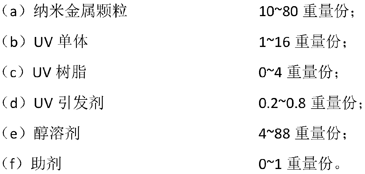
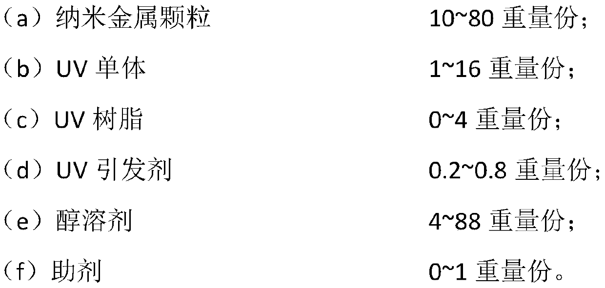
[0074] (1) The dispersion liquid (60 weight parts of nano-silver particles, 8 weight parts of 4-hydroxybutyl acrylate (4-HBA) , 1 weight part of hyperbranched acrylic resin, isopropyl sulfide 0.4 parts by weight of xanthone (ITX), 30 parts by weight of ethylene glycol methyl ether, 0.4 parts by weight of leveling agent BYK 333, and 0.2 parts by weight of film-forming agent ethylene glycol phenyl ether) are evenly coated on the Polyethylene terephthalate (PET) film ( figure 1 Mark 1) in the surface, the coating thickness is 2 μm, and pre-dried at 50 ° C for 18 minutes to obtain a substrate coated with a nano-metal coating ( figure 1 Mark 2).
[0075] (2) the base material ( figure 1 Mark 2) to perform ultraviolet light exposure treatment to form a light-cured stereotyped conductive grid containing the nanometer metal with a grid line width of 6 μm, a horizontal grid line spacing of 120 μm, and a longitudinal grid line spacing of 120 μm ( figure 1 Mark 3). Rinse developed ex...
Embodiment 2
[0080] (1) Dispersion liquid (50 weight parts of nano-silver particles, 1 weight part of acryloyl morpholine (ACMO), 4 weight parts of polyester acrylate, 2,4,6-trimethyl 0.25 parts by weight of benzoyl-diphenylphosphine oxide (TPO), 43.75 parts by weight of propylene glycol ethyl ether, 0.2 parts by weight of leveling agent BYK333, 0.3 parts by weight of film-forming agent propylene glycol phenyl ether, and 0.5 parts by weight of adhesion promoter BYK4510 ) was uniformly coated on the glass surface by spraying method, the coating thickness was 4 μm, and pre-dried at 80° C. for 12 minutes to obtain a substrate coated with nano-silver coating.
[0081] (2) The base material coated with the nano-silver coating is subjected to ultraviolet light exposure treatment to form a grid line width of 3 μm, a horizontal grid line spacing of 150 μm, and a vertical grid line spacing of 150 μm containing the nano-metal. Light-cured shaped conductive mesh. Rinse and develop exposed transparen...
PUM
| Property | Measurement | Unit |
|---|---|---|
| thickness | aaaaa | aaaaa |
| thickness | aaaaa | aaaaa |
| width | aaaaa | aaaaa |
Abstract
Description
Claims
Application Information
 - R&D
- Intellectual Property
- Life Sciences
- Materials
- Tech Scout
- Unparalleled Data Quality
- Higher Quality Content
- 60% Fewer Hallucinations
Browse by: Latest US Patents, China's latest patents, Technical Efficacy Thesaurus, Application Domain, Technology Topic, Popular Technical Reports.
© 2025 PatSnap. All rights reserved.Legal|Privacy policy|Modern Slavery Act Transparency Statement|Sitemap|About US| Contact US: help@patsnap.com