Preparation method of GaN-based low-order surface grating DFB laser

A technology of DFB lasers and surface gratings, applied in lasers, semiconductor lasers, phonon exciters, etc., can solve the problems of high cost, small grating area, large-area device preparation, etc., and achieve high side mode suppression ratio and single mode selection Good performance, improve the effect of uniformity

Inactive Publication Date: 2019-03-12
INST OF ELECTRONICS ENG CHINA ACAD OF ENG PHYSICS
View PDF7 Cites 5 Cited by
  • Summary
  • Abstract
  • Description
  • Claims
  • Application Information

AI Technical Summary

Problems solved by technology

For GaN-based DFB lasers, the grating period is about a hundred nanometers. One of the usual methods is electron beam exposure, but the grating area prepared by this method is small. If a large-area grating at the epitaxial wafer level is prepared, the electron beam exposure will take a long time. , the splicing accuracy of the writing field is difficult to guarantee, and the cost is too high; or a short-period grating structure is prepared by means of deep ultraviolet laser double-beam interference exposure. After exposure and development, the grating pattern is transferred to the semiconductor material by chemical etching or reactive ion etching. , but deep ultraviolet lithography has high requirements on the performance of the lithography machine
[0005] In short, the existing embedded grating DFB laser has the problem of difficult material regrowth, resulting in low yield and high cost
Moreover, the existing surface grating DFB lasers have problems such as high equipment requirements, high cost and inability to prepare large-area devices.
The above problems are also bottlenecks that limit the mass use of GaN-based DFB lasers

Method used


Image

  • Preparation method of GaN-based low-order surface grating DFB laser
  • Preparation method of GaN-based low-order surface grating DFB laser
  • Preparation method of GaN-based low-order surface grating DFB laser

Examples


Embodiment Construction

[0027] In order to further illustrate the technical means and functions adopted by the present invention to achieve the purpose of the invention, the specific implementation manners of the present invention will be described below in conjunction with the drawings. The following examples serve to illustrate the invention, but do not limit the scope of the invention.

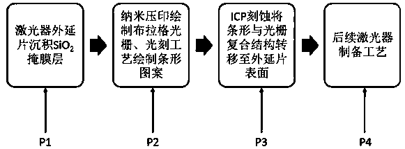
[0028] The preparation method of the GaN-based low-order surface grating DFB laser proposed by the present invention, such as figure 1 shown, including the following steps:

[0029] Step P1, prepare the GaN-based laser epitaxial wafer, use acetone, alcohol and deionized water to ultrasonically clean and then use PECVD to deposit SiO 2 The mask is used as the substrate for backup;

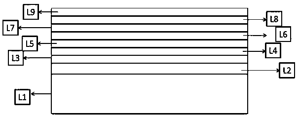
[0030] Its structure is as figure 2 As shown, the substrate used for the epitaxial wafer is an N-type GaN self-supporting substrate, and the lower confinement layer, the lower waveguide layer, the multi-quantum well active layer, th...


PUM

PropertyMeasurementUnit
reflectanceaaaaaaaaaa

Abstract

The invention discloses a preparation method of a GaN-based low-order surface grating DFB laser. The method comprises the following steps: depositing a SiO2 mask on an epitaxial wafer of the GaN-basedlaser; preparing uniform Bragg gratings on the surface of the substrate by using a nanoimprint technique, fabricating strip patterns by photolithography, and forming a composite structure of ridges and gratings; etching the GaN, and etching the epitaxial wafer through a strip photoresist and the grating SiO2 composite structure mask to form a surface composite grating structure having ridges; andpreparing upper and lower electrode structures of a laser chip to obtain a GaN-based DFB semiconductor laser. The method etches the ridge patterns required by the grating preparation and at the laterstage of the process at the same time, and combines the nano imprint template and the lithography pattern design respectively, which can design and prepare GaN-based DFB lasers with different wavelengths, different order gratings and different sizes, and can greatly reduce the cost of GaN-based DFB semiconductor lasers and effectively improve the uniformity of products.

Description

technical field [0001] The invention belongs to the field of semiconductor optoelectronic devices, relates to a GaN-based DFB semiconductor laser, in particular to a preparation method of a GaN-based low-order surface grating DFB laser. Background technique [0002] Information transmission requires a stable single-mode laser, and this application requirement promotes the research and development of semiconductor lasers. When a semiconductor laser is used as a light source in a communication system, if it has dispersion, the spectral broadening will reduce the transmission bandwidth, thereby limiting the transmission rate. Distributed feedback (DFB) semiconductor laser is the core device of the transmitting end in the optical communication system. The Bragg grating is used to effectively select the resonant mode. The resonant cavity loss of different wavelengths of lasers is quite different, so it can still maintain complete singleness in the case of high-speed modulation. ...

Claims


Application Information

Patent Timeline
Patent Type & Authority Applications(China)
IPC IPC(8): H01S5/34H01S5/12
CPCH01S5/12H01S5/34333
Inventor 李俊泽张建邓泽佳杨浩军李沫
Owner INST OF ELECTRONICS ENG CHINA ACAD OF ENG PHYSICS
Why Eureka
Try Eureka