
Processing method for silicon carbide gate-dielectric fluorine plasma and silicon carbide power device

A technology of fluorine plasma and silicon carbide gate, which is applied in the direction of semiconductor devices, semiconductor/solid-state device manufacturing, electrical components, etc., can solve the problems of increasing manufacturing costs and difficulties, avoid toxic gases and high-temperature processes, and achieve good dielectric morphology , the effect of improving reliability

Active Publication Date: 2019-03-26
北京国联万众半导体科技有限公司
View PDF8 Cites 0 Cited by
  • Summary
  • Abstract
  • Description
  • Claims
  • Application Information

AI Technical Summary

Problems solved by technology

The gas used in the traditional annealing process is mostly toxic gas, and it needs to be carried out in a specific oxidation furnace. The oxidation temperature is as high as 1300 ° C and above, which increases the cost and difficulty of the process preparation

Method used


Image

  • Processing method for silicon carbide gate-dielectric fluorine plasma and silicon carbide power device
  • Processing method for silicon carbide gate-dielectric fluorine plasma and silicon carbide power device
  • Processing method for silicon carbide gate-dielectric fluorine plasma and silicon carbide power device

Examples


specific Embodiment approach

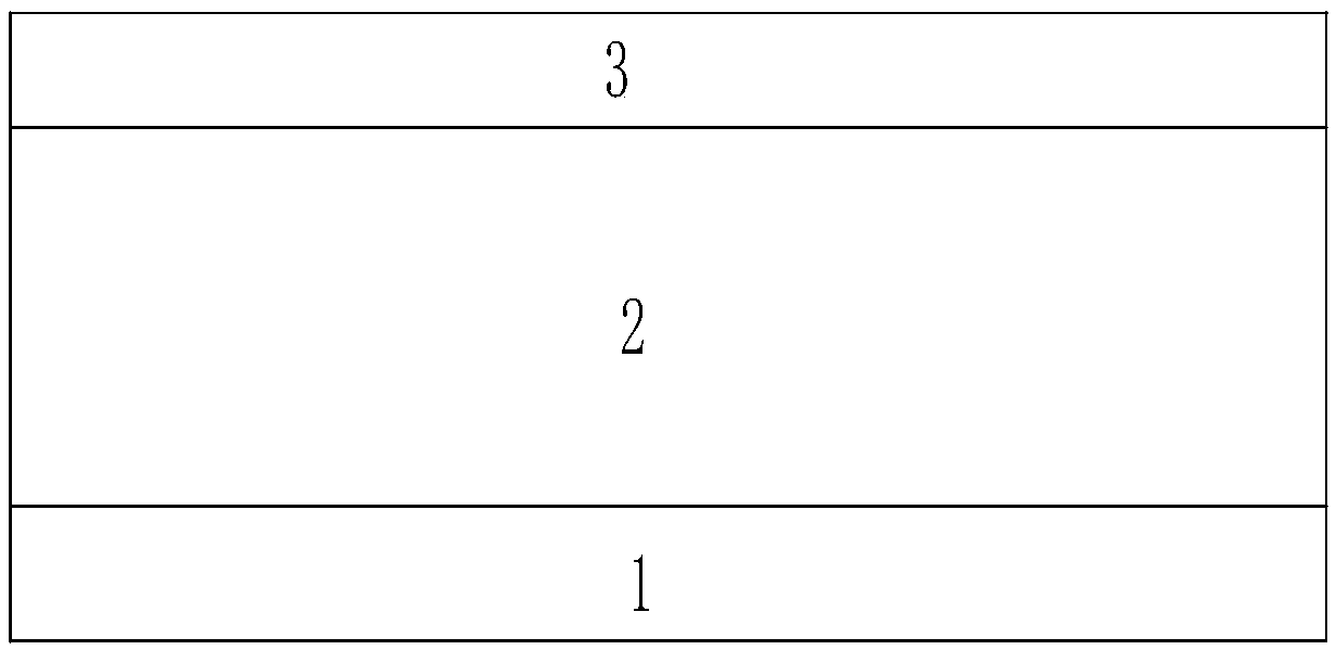
[0043] see image 3 , as a specific implementation of the silicon carbide gate dielectric fluorine plasma treatment method provided by the present invention, the oxidation process is carried out in an oxidation furnace, the oxidation temperature does not exceed 1200°C, and the oxidation time is 100min-150min.

[0044] Optionally, the oxidation temperature does not exceed 1100° C., and the oxidation time is 110 min-130 min.

[0045] Optionally, the oxidation temperature is 1000° C., and the oxidation time is 120 minutes.

Embodiment approach

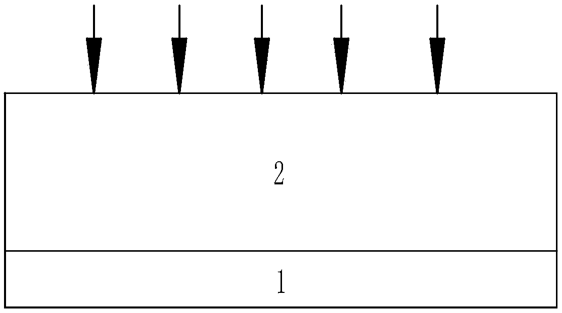
[0046] refer to figure 1 , as a specific implementation of the silicon carbide gate dielectric fluorine plasma treatment method provided by the present invention, the wafer includes silicon carbide N + Substrate 1 and SiC N - Epitaxial layer 2.

[0047] see figure 1 , as a specific implementation of the silicon carbide gate dielectric fluorine plasma treatment method provided by the present invention, the wafer is cleaned by the RCA cleaning method, and the RCA cleaning method mainly includes:

[0048] First use acidic hydrogen peroxide containing sulfuric acid for acidic oxidation cleaning;

[0049] Then use amine-containing weak alkaline hydrogen peroxide for alkaline oxidation cleaning;

[0050] Then wash with dilute hydrofluoric acid solution;

[0051] Finally, acidic oxidation cleaning is carried out with acidic hydrogen peroxide containing hydrochloric acid;

[0052] Rinse with ultrapure water between each cleaning, and finally dry with low-boiling organic solvents...


PUM


Abstract

The invention provides a processing method for silicon carbide gate-dielectric fluorine plasma and a silicon carbide power device. The method comprises: cleaning a wafer; carrying out electron cyclotron resonance- fluorine plasma treatment on the surface of the cleaned wafer; and placing the processed wafer in an oxidizing furnace to carry out oxidation. According to the processing method providedby the invention, since the fluorine-contained plasma treatment is carried out before dry-oxygen oxidation of the silicon carbide and silicon carbide oxidization of the processed silicon carbide is realized in a low-temperature oxidation device, the usage of toxic gas in the traditional annealing process is avoided and the usage of specific high-temperature oxidation annealing equipment is avoided, so that the gate dielectric reliability is ensured, the costs of the process and equipment are lowered, and the thermal budget of the process is reduced.

Description

technical field [0001] The invention belongs to the technical field of semiconductor devices, and more specifically relates to a method for processing silicon carbide gate dielectric fluorine plasma and a silicon carbide power device. Background technique [0002] The third-generation semiconductor materials represented by silicon carbide (SiC) have superior properties such as large bandgap, high critical field strength, and high thermal conductivity. They are one of the ideal materials for preparing high-voltage, high-power, and radiation-resistant devices. Ability to directly grow SiO by thermal oxidation 2 The advantage of the medium has accelerated the development of SiC MOSFET devices (MOSFET is the abbreviation of Metal-Oxide-Semiconductor Field-Effect Transistor, Metal-Oxide-Semiconductor Field-Effect Transistor, referred to as Metal-Oxide Semiconductor Field-Effect Transistor). SiO 2 The interface quality of the gate dielectric is very poor, SiC / SiO 2 High interfa...

Claims


Application Information

Patent Timeline
Patent Type & Authority Applications(China)
IPC IPC(8): H01L21/324H01L29/16H01L29/423
CPCH01L21/3247H01L29/1608H01L29/42364
Inventor 刘佳佳樊帆高渊毕胜赢崔玉兴
Owner 北京国联万众半导体科技有限公司
Features
  • Generate Ideas
  • Intellectual Property
  • Life Sciences
  • Materials
  • Tech Scout
  • Unparalleled Data Quality
  • Higher Quality Content
  • 60% Fewer Hallucinations
Learn More