Silicon carbide crystal and method for manufacturing the same
一种碳化硅、晶体的技术,应用在化学仪器和方法、半导体/固态器件制造、晶体生长等方向,能够解决SiC晶体成长速度缓慢、制程控制困难、复杂等问题,达到降低缺陷密度与残留应力的效果
- Summary
- Abstract
- Description
- Claims
- Application Information
AI Technical Summary
Problems solved by technology
Method used
Image

Examples
Embodiment 1
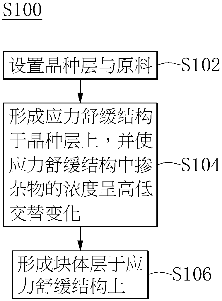
[0024] see figure 1 As shown, the manufacturing method S100 of the silicon carbide crystal of the present invention includes: step S102, setting a seed layer and raw materials; step S104, forming a stress relief structure on the seed layer, and making the concentration of the dopant in the stress relief structure to be alternating high and low; and step S106 , forming a bulk layer on the stress relief structure.
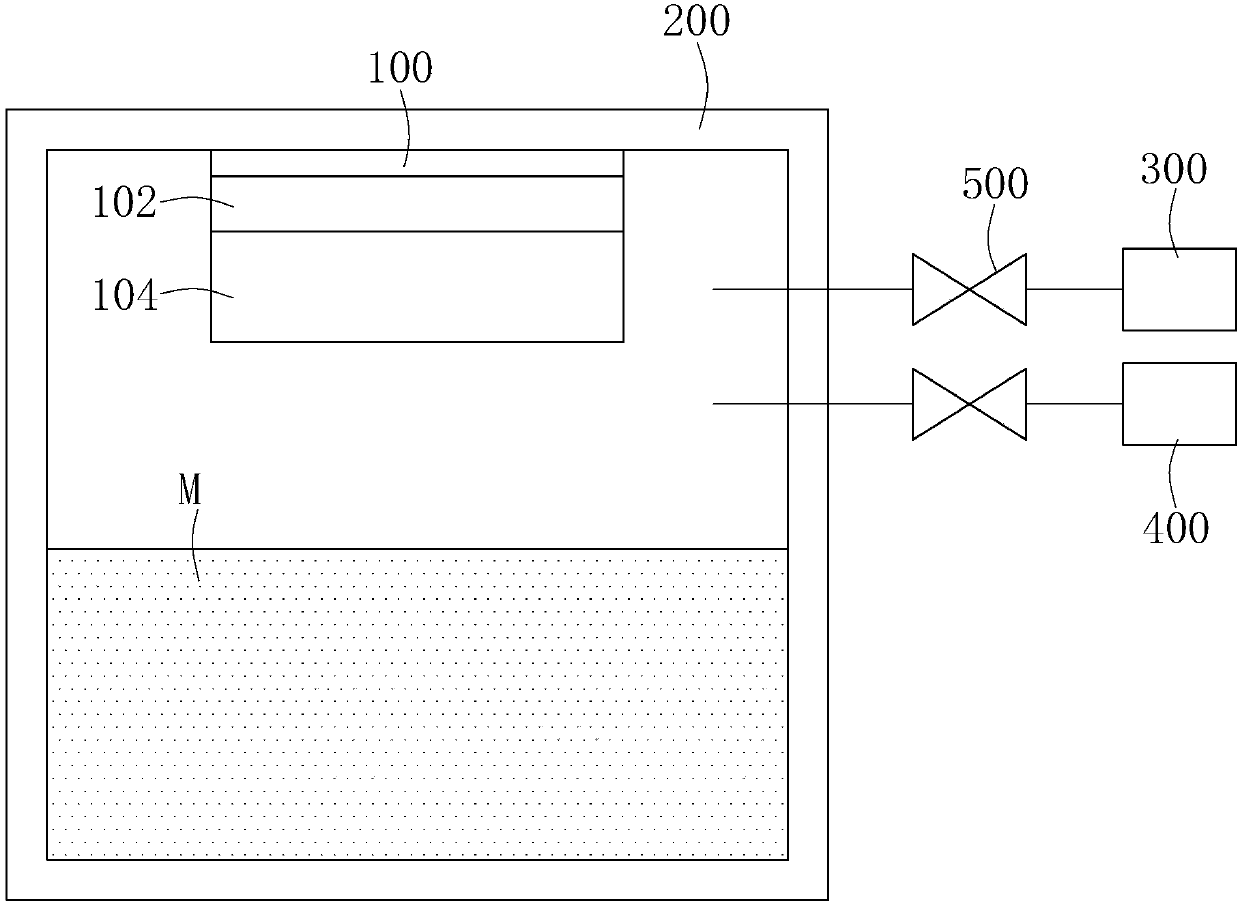
[0025] In step S102, please refer to figure 2 As shown, the seed layer 100 can be placed in the reactor 200 opposite to the raw material M, for example, the seed layer 100 is placed on the top of the reactor 200 and the raw material M is placed at the bottom of the reactor 200 . The seed layer 100 can be a SiC seed layer, and the material M can be a solid material that can provide Si and C elements required for crystal growth, such as SiC powder or a mixture of Si particles and carbon powder. In addition, the reactor 200 may use a graphite crucible, and the periph...
Embodiment 2
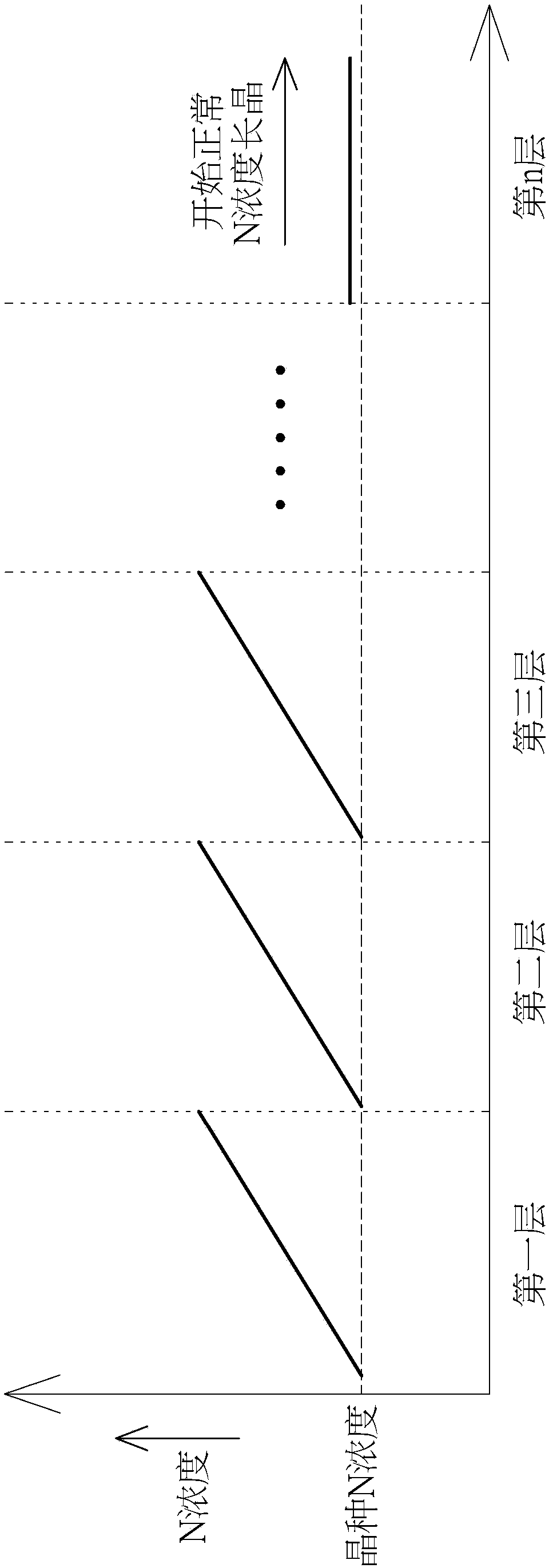
[0035] see Figure 5A and Figure 5B As shown, it shows another embodiment in which the concentration of the dopant changes alternately from high to low in step S104. The difference between this embodiment and Embodiment 1 is that the concentration of the dopant is repeatedly controlled between a first concentration greater than the concentration of the dopant in the seed layer 100 and a concentration lower than the concentration of the dopant in the seed layer 100 The second concentration increases or decreases continuously; if the concentration of the dopant in the seed layer 100 is regarded as the reference concentration, the concentration of the dopant in the stress relief structure 102 described in this embodiment changes alternately. , which means that the concentration of the dopant is repeatedly increased over a period of time from the second concentration to the first concentration (such as Figure 5A shown), or a continuous decrease from the first concentration to ...
Embodiment 3
[0038] see Figure 6A and Figure 6B As shown in FIG. 1 , it shows another embodiment in which the concentration of the dopant changes alternately from high to low in step S104 . The difference between this embodiment and the above-mentioned embodiments is that a first concentration greater than the concentration of the dopant in the seed layer and a concentration of the dopant in the seed layer are applied alternately, or a first concentration greater than the concentration of the dopant in the seed layer is alternately applied. The dopant concentration is a first concentration and a second concentration less than the dopant concentration in the seed layer. If the concentration of the dopant in the seed layer 100 is regarded as the reference concentration, the way in which the concentration of the dopant in the stress relief structure 102 described in this embodiment changes alternately means that the concentration of the dopant changes over a period of time. The concentrat...
PUM
| Property | Measurement | Unit |
|---|---|---|
| band gap | aaaaa | aaaaa |
Abstract
Description
Claims
Application Information
 - R&D
- Intellectual Property
- Life Sciences
- Materials
- Tech Scout
- Unparalleled Data Quality
- Higher Quality Content
- 60% Fewer Hallucinations
Browse by: Latest US Patents, China's latest patents, Technical Efficacy Thesaurus, Application Domain, Technology Topic, Popular Technical Reports.
© 2025 PatSnap. All rights reserved.Legal|Privacy policy|Modern Slavery Act Transparency Statement|Sitemap|About US| Contact US: help@patsnap.com