A testing device and method for a thin-film electrode of a solid oxide fuel cell
A solid oxide and thin film electrode technology, applied in the field of electrochemical testing, can solve the problems of difficulty in meeting the testing requirements of medium and high temperature solid oxide cathode thin film materials, and not equipped with probes for electrochemical performance testing, so as to prevent damage to current collectors. Layers, space-saving, evenly distributed effects
- Summary
- Abstract
- Description
- Claims
- Application Information
AI Technical Summary
Problems solved by technology
Method used
Image
Examples
Embodiment 1
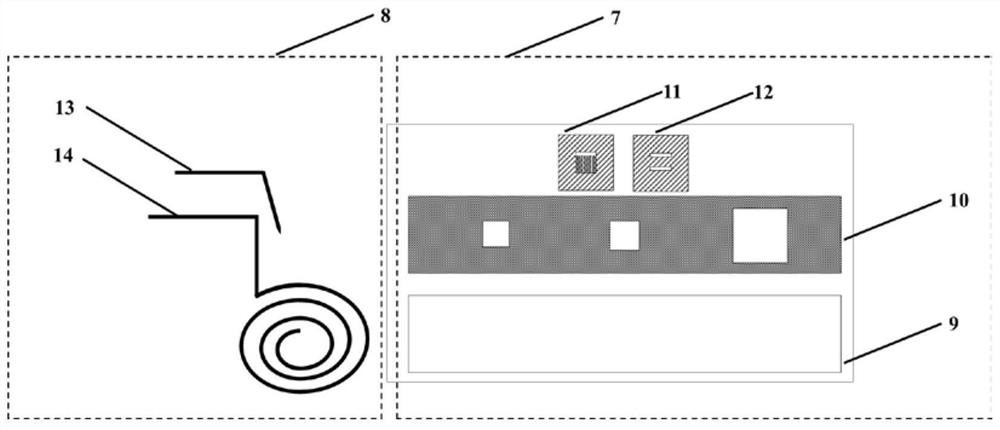
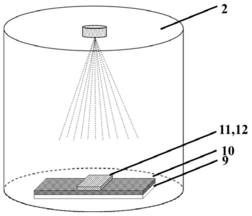
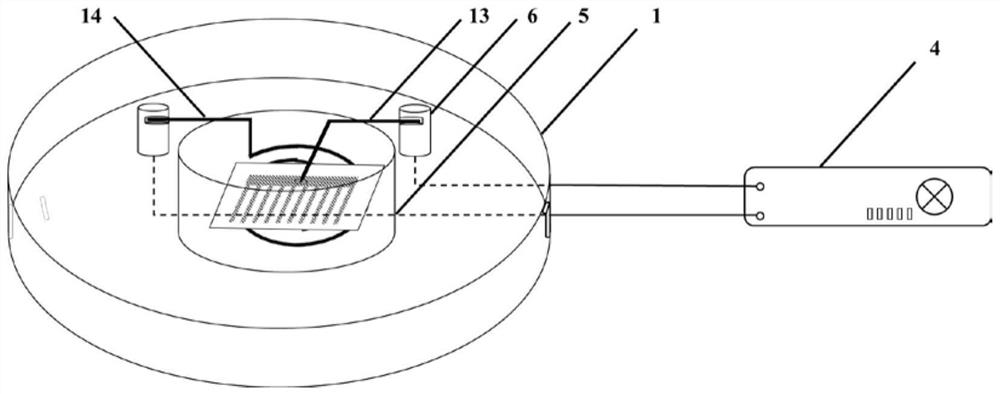
[0058] 1) Fix the comb-shaped hollow mask 11 above the 5mm*5mm snap hole in the middle of the front of the clip 10 with conductive glue, and prepare a thin film sample Nd with a size of 5mm*5mm*1mm prepared by the pulsed laser deposition method. 0.5 Sr 0.5 CoO 3-δ -Zr 0.92 Y 0.08 o 2 (hereinafter referred to as NSC-YSZ) from the back of the clamping piece 10 into the clamping hole in the middle of the clamping piece, so that the sample surface is facing the mask side, and the glass bottom plate 9 is assembled; the collector layer spraying mold 7 is placed upwards. Put it into the gold spray tank 2, spray a layer of comb-shaped gold collector layer with a thickness of about 100nm on the surface of the film NSC-YSZ, the sputtering current is 5mA, and the total sputtering time is 100s;
[0059] 2) Apply a layer of platinum slurry evenly on the bottom of the film material NSC-YSZ, the thickness is about 0.3-0.5mm, and apply a little platinum slurry on the center of the comb ha...
Embodiment 2
[0063] 1) Fix the strip-shaped hollow mask 12 with conductive glue above the 5mm*5mm snap hole in the middle of the front of the snap-in sheet 10, and prepare a film sample Nd with a size of 4mm*4mm*1mm prepared by the pulsed laser deposition method. 0.5 Sr 0.5 CoO 3-δ -SrTiO 3 (hereinafter referred to as NSC-STO), from the back of the card position piece 10 into the card position hole of the corresponding size on the card position piece, so that the sample surface faces the mask side, and the glass bottom plate 9 is assembled; the collector layer spraying mold 7 faces Put it into the gold spray tank 2, and spray two strips of comb-shaped gold collector layers with a thickness of about 100nm on the surface of the thin film NSC-YSZ. The sputtering current is 5mA, and the total sputtering time is 100s; take out the collector layer Spray the thin film electrode sample in the mold, apply a little platinum slurry on the center of the two strip-shaped current collectors on the upp...
Embodiment 3
[0067] The difference between this embodiment and embodiment 2 is that the film sample tested is La 0.6 Sr 0.4 CoO 3-δ -SrTiO 3 (hereinafter referred to as LSC-STO), when conducting electrical tests, the temperature is stabilized at 700°C, and a mixed gas with an oxygen partial pressure of 10% is stably introduced into the heating chamber first, and the resistance value of the sample is recorded, and then through the three-way valve Quickly switch to a mixed gas with an oxygen partial pressure of 1%, record the change in the resistance value during this process until the resistance is stable again, record 1 point per second during the test, and the test results are as follows: Figure 7 shown. According to this test result, combined with the conductance relaxation method formula, the oxygen exchange rate on the surface of the thin film sample can be calculated.
PUM
| Property | Measurement | Unit |
|---|---|---|
| length | aaaaa | aaaaa |
| length | aaaaa | aaaaa |
| diameter | aaaaa | aaaaa |
Abstract
Description
Claims
Application Information


