Graphene surface plasmon devices, surface plasmon waveguides and optoelectronic devices

A graphene surface and plasmon excitation technology, applied in the field of infrared light detection, can solve problems such as dynamic regulation of graphene plasmons that have not been mentioned

Active Publication Date: 2021-08-27
CHONGQING INST OF GREEN & INTELLIGENT TECH CHINESE ACADEMY OF SCI
View PDF9 Cites 0 Cited by
  • Summary
  • Abstract
  • Description
  • Claims
  • Application Information

AI Technical Summary

Problems solved by technology

However, none of these mentioned the dynamic control of graphene plasmons. Therefore, there is an urgent need for a graphene surface plasmon device that can dynamically control plasmons.

Method used


Image

  • Graphene surface plasmon devices, surface plasmon waveguides and optoelectronic devices
  • Graphene surface plasmon devices, surface plasmon waveguides and optoelectronic devices
  • Graphene surface plasmon devices, surface plasmon waveguides and optoelectronic devices

Examples


Embodiment 1

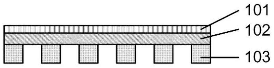
[0036] see figure 1 , is a schematic structural diagram of an embodiment of a graphene surface plasmon waveguide of the present invention. Specifically, the graphene surface plasmon waveguide of this embodiment includes conductive A capacitor-like structure composed of a periodic scatterer 103, a dielectric layer 102 and a graphene layer 101, wherein,

[0037] The graphene layer 101 is a single layer or two layers of continuous graphene without nano-patterning, with a size of 100 μm×100 μm (of course, the size of the graphene layer can be adjusted according to the actual size of the waveguide);

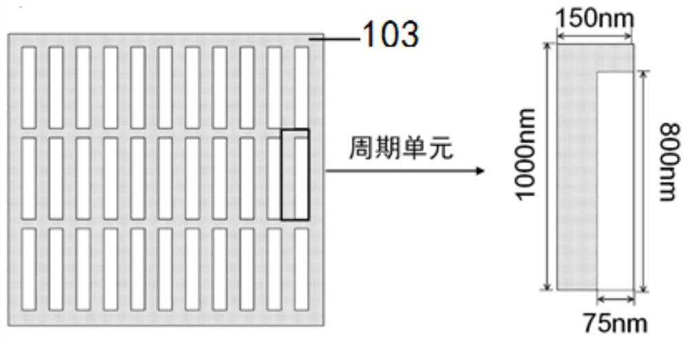
[0038] The dielectric layer 102 is made of aluminum oxide with a thickness of 5nm; the conductive periodic scatterer 103 is made of two-dimensional conductive grating layer and made of 80nm thick gold; specifically, see figure 2 , the two-dimensional conductive grating 103 is composed of periodic rectangular holes with a period of 1000nm×150nm, wherein the size of the rectangular ho...

Embodiment 2

[0043] The present invention also provides another graphene surface plasmon waveguide, the structure of which is the same as that of the above-mentioned embodiment, both including a conducting conductive periodic scatterer 103 and a graphene layer 101, and a conductive periodic scattering The dielectric layer 102 between the body 103 and the graphene layer 101, the difference is that in this embodiment,

[0044] The graphene layer 101 is three-layer / fifteen-layer graphene, and each layer is continuous graphene without nano-patterning;

[0045] The dielectric layer 102 is made of multilayer two-dimensional boron nitride with a thickness of 15nm;

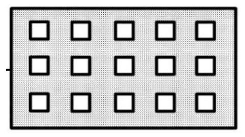
[0046] The conductive periodic scatterer 103 adopts a two-dimensional conductive grating layer, which is made of indium tin oxide with a thickness of 300nm, and the first period is 250nm, the period unit is a square hole, and the side length of the hole is 70nm, see image 3 .

[0047] Of course, in this embodiment, the periodic uni...

Embodiment 3

[0049] The present invention also provides a graphene surface plasmon waveguide, which includes the structure of the above-mentioned embodiment 1 or embodiment 2, the difference is, see Figure 5 , The graphene surface plasmon waveguide in this embodiment also includes a reflection enhancement layer 104 located below the conductive periodic scatterer, specifically, the reflection enhancement layer 104 sequentially includes from top to bottom:

[0050] A cavity length control layer 1041 made of potassium bromide with a thickness of 1.5 μm; and a reflective layer 1042 made of silver with a thickness of 100 nm.

[0051] In this embodiment, a resonant cavity is formed by the cavity length control layer and the reflection layer, that is, the reflection enhancement layer.

[0052] Further, in order to enhance the adhesion between the reflective layer 1042 and the substrate in the optoelectronic device, titanium with a thickness of 5 nm is disposed under the reflective layer 1042 to ...


PUM

PropertyMeasurementUnit
thicknessaaaaaaaaaa
thicknessaaaaaaaaaa
thicknessaaaaaaaaaa

Abstract

The invention discloses a graphene surface plasmon device, which includes a capacitor-like structure formed by a conductive periodic scatterer-dielectric layer-graphene layer, so that the conductive periodic scatterer, such as one-dimensional / two-dimensional Conductive gratings are used to increase the wave vector of free-space light to match the wave vector of graphene conduction-type plasmons to excite graphene conduction-type plasmons; The electron concentration of graphene can be adjusted by applying voltage between the periodic scatterers, so as to realize the dynamic regulation of graphene surface plasmons, that is, the conductive periodic scatterers not only serve as the excitation structure of graphene plasmons, At the same time, it is also used as an electrode for the regulation of graphene electron concentration to realize the dynamic regulation of graphene surface plasmons. Correspondingly, the present invention also provides a graphene surface plasmon waveguide and a corresponding optoelectronic device.

Description

technical field [0001] The invention relates to the technical field of infrared light detection, in particular to a graphene surface plasmon device, a graphene surface plasmon waveguide, and an optoelectronic device. Background technique [0002] As a cutting-edge branch of nanophotonics, plasmonics mainly studies how to use surface plasmons to realize the generation, transmission and manipulation of optical signals at the nanoscale. Surface plasmon (Surface Plasmon, SP) is a new electromagnetic mode formed by the interaction of electromagnetic waves and plasma oscillations in the surface area of ​​conductors. Surface plasmons can exist in zero-dimensional, one-dimensional, and two-dimensional systems: in zero-dimensional systems, such as spherical nanoparticles, surface plasmons are bound by the three coordinates of x, y, and z, called It is a localized surface plasmon; the surface plasmon in a one-dimensional system, such as a nanowire, and a two-dimensional system, such ...

Claims


Application Information

Patent Timeline
Patent Type & Authority Patents(China)
IPC IPC(8): G02B5/00G02B6/122G02F1/01
Inventor 汤林龙
Owner CHONGQING INST OF GREEN & INTELLIGENT TECH CHINESE ACADEMY OF SCI
Why Eureka
Try Eureka