Micro-cavity discharge ultraviolet radiation device and preparation method thereof, and micro-cavity array based on micro-cavity discharge ultraviolet radiation device
A technology of ultraviolet radiation and microcavity discharge, applied in the direction of discharge tubes, electrical components, circuits, etc., can solve the problems of small irradiation field of view, low uniformity of irradiation, environmental pollution, etc., and achieve high-precision results
- Summary
- Abstract
- Description
- Claims
- Application Information
AI Technical Summary
Problems solved by technology
Method used
Image


Examples
Embodiment 1
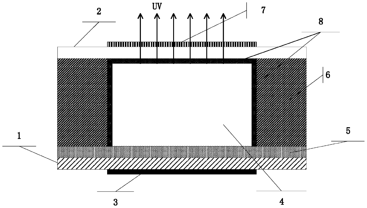
[0052] see figure 1 , is a schematic diagram of the structure of a microcavity discharge ultraviolet radiation device, including a substrate 1, a bottom electrode 3, a dielectric layer 5, a microcavity cavity 4, a barrier 6 and a phosphor layer 8 (different phosphor materials can be used to obtain different targets) spectral line), dielectric plate 2 and top electrode 7. The bottom electrode 3 is a gold electrode, the substrate 1 is a silicon substrate, the dielectric layer 5 is a magnesium oxide layer, the barrier wall 6 is made of polyester material SU-8, the phosphor layer 8 is made of a rare earth material, the dielectric plate 2 is made of glass, and the top electrode 7 Indium tin oxide (ITO) is used.
[0053] The method for preparing a microcavity ultraviolet radiation device specifically comprises the following steps:
[0054] (1) Clean the silicon substrate: use acetone, isopropanol and deionized water to ultrasonically clean the silicon substrate for 5 minutes each,...
Embodiment 2
[0064] see figure 2 , is a schematic diagram of a cuboid microcavity regular array (the numbers of rows and columns of the microcavity array are respectively M and N; wherein M, N=1,2,3,...10 5 ), the length, width, and height of the microcavity are a, b, and c, respectively, and the ranges of a, b, and c are all from 1 μm to 10 4 μm. The device structure includes a substrate, a bottom electrode, a dielectric layer, a microcavity, a barrier, a phosphor layer (using different phosphor materials, different target band spectral lines can be obtained), a dielectric plate, and a top electrode; the bottom electrode is a gold electrode , the substrate is a silicon substrate, the dielectric layer is a magnesium oxide layer, the barrier wall is SU-8, the phosphor layer is a rare earth material, the dielectric plate is glass, and the top electrode is indium tin oxide (ITO).
Embodiment 3
[0066] see image 3 , is a schematic diagram of an irregular array of cylindrical microcavities. The depth of the microcavity is h, where h ranges from 1 μm to 10 4 μm, the cavity diameter is d, where d ranges from 1 μm to 10 4 μm. The device structure includes a substrate, a bottom electrode, a dielectric layer, a microcavity, a barrier, a phosphor layer (using different phosphor materials, different target band spectral lines can be obtained), a dielectric plate, and a top electrode; the bottom electrode is a gold electrode , the substrate is a silicon substrate, the dielectric layer is a magnesium oxide layer, the microcavity barrier is SU-8, the phosphor layer is a rare earth material, the dielectric plate is glass, and the top electrode is indium tin oxide (ITO).
PUM
| Property | Measurement | Unit |
|---|---|---|
| Thickness | aaaaa | aaaaa |
| Thickness | aaaaa | aaaaa |
Abstract
Description
Claims
Application Information