Eureka AIR delivers breakthrough ideas for toughest innovation challenges, trusted by R&D personnel around the world.

Diffusion method suitable for selective emitter

A diffusion method and emitter technology, applied in photovoltaic power generation, climate sustainability, electrical components, etc., can solve problems such as unsatisfactory contact performance, expensive special paste, technical potential bottlenecks, etc., and achieve an increase in short-circuit current Isc , Improve the open circuit voltage, good effect of square resistance uniformity

Active Publication Date: 2019-05-21
HANWHA SOLARONE QIDONG
View PDF6 Cites 7 Cited by
  • Summary
  • Abstract
  • Description
  • Claims
  • Application Information

AI Technical Summary

Problems solved by technology

[0004] At present, for solar cells formed on the basis of p-type silicon wafers, the technology for preparing front surface emitters is mainly POCl 3 Diffusion method, the technical potential of this method has gradually become a bottleneck with the increase in the need to prepare high-resistance emitters. Of course, although a few manufacturers have obtained in the process of preparing emitter crystalline silicon cells with a square resistance above 100Ω / □ Breakthrough, but its special slurry is relatively expensive, and the contact performance is not satisfactory, and the efficiency has no advantage

Method used


Image

  • Diffusion method suitable for selective emitter

Examples


Embodiment 1

[0056] A diffusion method suitable for selective emitters in this embodiment includes the following steps:

[0057] Step 1: First Surface Deposition

[0058] The temperature of the furnace tube is raised to 800°C, and a mixed gas consisting of small nitrogen, large nitrogen and oxygen carrying phosphorus oxychloride is introduced into the furnace tube. The flow rate of the small nitrogen is 500 sccm, the flow rate of the large nitrogen is 800 sccm, and the flow rate of the oxygen is 600 sccm with a step run time of 12 min.

[0059] Step 2: First drive into

[0060] Raise the temperature of the furnace tube to 880°C, and feed large nitrogen, oxygen and small nitrogen gas into the furnace tube, so that the phosphorus source deposited on the surface of the silicon wafer can be driven and diffused into the silicon wafer at high temperature, and the flow rate of the large nitrogen gas is 800 sccm , the small nitrogen gas flow rate is 500 sccm, the oxygen gas flow rate is 300 sccm...

Embodiment 2

[0077] A diffusion method suitable for selective emitters in this embodiment includes the following steps:

[0078] Step 1: First Surface Deposition

[0079] The temperature of the furnace tube is raised to 790°C, and a mixed gas composed of large nitrogen, oxygen and small nitrogen carrying phosphorus oxychloride is introduced into the furnace tube. The flow rate of the small nitrogen is 400 sccm, the flow rate of the large nitrogen is 700 sccm, and the flow rate of the oxygen is 500sccm, the time of passing gas is 11min.

[0080] Step 2: First drive into

[0081] Raise the temperature of the furnace tube to 870°C, and feed large nitrogen, oxygen, and small nitrogen gases into the furnace tube, so that the phosphorus source deposited on the surface of the silicon wafer can be driven and diffused into the silicon wafer at high temperature, and the flow rate of the large nitrogen gas is 700sccm , the flow rate of oxygen gas is 200 sccm, the flow rate of small nitrogen gas is ...

Embodiment 3

[0095] A diffusion method suitable for selective emitters in this embodiment includes the following steps:

[0096] Step 1: First Surface Deposition

[0097] The temperature of the furnace tube is raised to 810°C, and a mixed gas composed of large nitrogen, oxygen and small nitrogen carrying phosphorus oxychloride is introduced into the furnace tube. The flow rate of the small nitrogen is 600 sccm, the flow rate of the large nitrogen is 900 sccm, and the flow rate of the oxygen is 700sccm, the time of passing gas is 13min.

[0098] Step 2: First drive into

[0099] Raise the temperature of the furnace tube to 890°C, and feed large nitrogen, oxygen, and small nitrogen gas into the furnace tube, so that the phosphorus source deposited on the surface of the silicon wafer can be driven and diffused into the silicon wafer at high temperature, and the flow rate of the large nitrogen gas is 900sccm , the flow rate of oxygen gas is 400 sccm, the flow rate of small nitrogen gas is 60...


PUM


Abstract

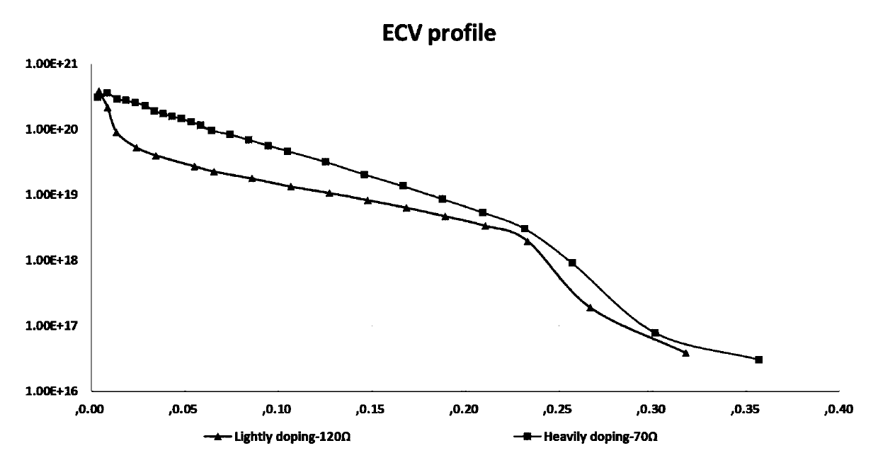
The invention discloses a diffusion method suitable for a selective emitter. The diffusion method comprises multi-time deposition and multi-time driving, and a temperature in a furnace tube begins tobe lowered from the second step of first-time driving. By use of a three-step diffusion deposition and driving way used by the invention, a PSG (Phosphosilicate Glass) layer containing high phosphorusconcentration is formed on the surface of a silicon wafer so as to be favorable for pushing a phosphorus source in the PSG into the silicon wafer during heavy doping, and a high-concentration heavy doping zone is formed so as to be favorable for ohmic contact to improve an FF (Fill Factor); the relative concentration of a shallow doping zone without heavy doping is low so as to be favorable for improving open-circuit voltage; a driving process capable of gradually lowering the temperature forms gradient doping in the silicon wafer, the width of a P-N shallow junction zone is widened, open-circuit voltage is improved, meanwhile, a shallow junction corresponds to a short wave band spectrum in sunlight, the spectrum in the range contains a large photon number, a better blue wave response canbe obtained, so that short circuit current Isc is improved, and in addition, sheet resistance uniformity is good due to the driving process capable of gradually lowering the temperature.

Description

technical field [0001] The invention relates to the technical field of solar cell manufacturing, in particular to a diffusion method suitable for a selective emitter. Background technique [0002] Solar photovoltaic power generation, due to its clean, safe, convenient and high-efficiency characteristics, has become an emerging industry that is widely concerned and focused on development all over the world. Therefore, the production of crystalline silicon solar cells has developed rapidly in recent years, and the demand for photovoltaic power plants and distributed applications is also very large. [0003] After more than ten years of industrial development of solar cells, its process has gradually matured and optimized, and diffusion is the core step of the manufacturing process, and the improvement of its process directly affects the improvement of battery efficiency. [0004] At present, for solar cells formed on the basis of p-type silicon wafers, the technology for prep...

Claims


Application Information

Patent Timeline
Patent Type & Authority Applications(China)
IPC IPC(8): H01L31/18H01L21/225H01L31/068
CPCY02E10/547Y02P70/50
Inventor 张薛丹费存勇赵福祥崔钟亨
Owner HANWHA SOLARONE QIDONG
Why Eureka
Eureka Blog
Learn More