Organic single crystal spin valve and preparation method and application thereof

A spin valve, single crystal technology, applied in the fields of magnetic field controlled resistors, electromagnetic device manufacturing/processing, material selection, etc., can solve problems such as low yield rate, achieve high yield rate, strong universality, The effect of increasing the carrier spin diffusion length

Active Publication Date: 2019-08-02
INST OF CHEM CHINESE ACAD OF SCI
View PDF11 Cites 2 Cited by
  • Summary
  • Abstract
  • Description
  • Claims
  • Application Information

AI Technical Summary

Problems solved by technology

At the same time, the traditional preparation process of organic spin valve devices has extremely high requirements, and the yield rate is very low.

Method used


Image

  • Organic single crystal spin valve and preparation method and application thereof
  • Organic single crystal spin valve and preparation method and application thereof
  • Organic single crystal spin valve and preparation method and application thereof

Examples


preparation example 1、2

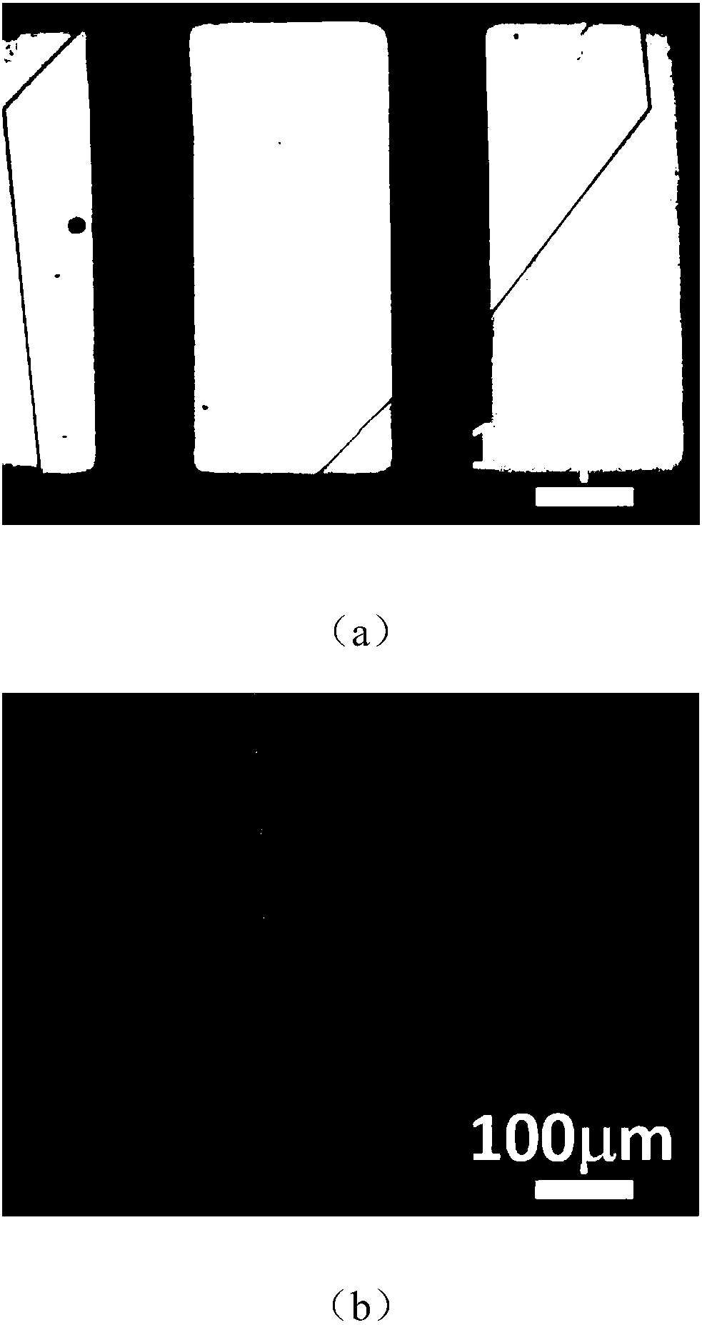
[0047] Preparation example 1, preparation of 2,6 diphenylanthracene (2,6-DPA) single crystal micron material

[0048] 1) Silicon wafer cleaning:

[0049] with SiO 2 Before use, the silicon wafer of the oxide layer should be cleaned with hydrogen peroxide:concentrated sulfuric acid (heated in an electric furnace, boiled) at a ratio of about 1:2, then ultrasonicated with deionized water, absolute ethanol and acetone for about 10 minutes, and finally used Dry quickly with nitrogen and place in an oxygen plasma generator for about 15 seconds.

[0050] 2) Silicon wafer surface modification

[0051] Place the cleaned silicon wafer in a petri dish in a vacuum drying oven, vacuumize and heat to 80°C for about 1 hour, keep the vacuum down to room temperature, and drop a small amount of n-octadecane near the silicon wafer in the petri dish Trichlorosilane (OTS), evacuated and heated to 120° C. for about 2 hours, and kept under vacuum to allow it to cool to room temperature. The modi...

Embodiment 1

[0056] 1. Preparation of lanthanum strontium manganese oxide (LSMO) ferromagnetic bottom electrode

[0057] 1.1) Patterned metal mask

[0058] A metal mask with a reasonable size can be customized according to the needs, and its patterned size determines the size of the lanthanum strontium manganese oxide (LSMO) ferromagnetic bottom electrode. The width here is preferably 500 μm.

[0059] 1.2) Preparation of lanthanum strontium manganese oxide (LSMO) ferromagnetic bottom electrode

[0060] Fix the patterned metal mask and the strontium titanate (STO) substrate, and put them into the DC facing target sputtering chamber. During the growth process, the substrate temperature is kept at 700-800°C, and the pressure in the chamber is about 0.5-1.0Pa, the carrier gas is the ratio Ar:O 2 = 5:3 mixture. After the epitaxial growth of 100nm-thick lanthanum strontium manganese oxide (LSMO) ferromagnetic electrode was completed, the pure O in situ at 3KPa 2 In the atmosphere, keep anne...

Embodiment 2

[0069] Embodiment 2 device performance test

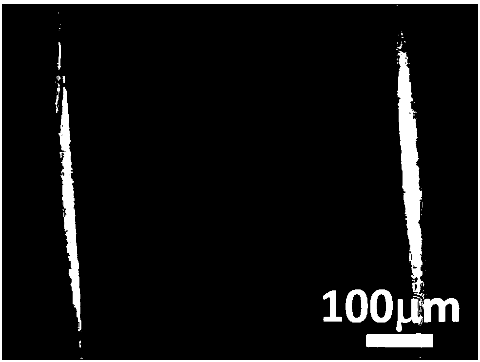
[0070] The 2,6-diphenylanthracene single crystal spin valve prepared in Example 1 was tested by Quantum Designed physical property measurement system (PPMS). Under an external 0.5T magnetic field, the magnetoresistance change is about 10% at 2K.

[0071] Figure 4 is the magnetoresistance curve (MR) of a 2,6 diphenylanthracene single crystal spin valve, given by Figure 4 It can be seen from the symmetrical MR curve that the spin single crystal spin valve device is successfully prepared, and the magnetoresistance change is about 10% at 2K.


PUM

PropertyMeasurementUnit
thicknessaaaaaaaaaa
thicknessaaaaaaaaaa
thicknessaaaaaaaaaa

Abstract

The invention discloses an organic single crystal spin valve and a preparation method and an application thereof. The organic single crystal spin valve includes a substrate, a ferromagnetic bottom electrode, an organic single crystal semiconductor micro / nano material, a buffer layer, a ferromagnetic top electrode and an oxidation protection layer. Because of the single structure and good crystal quality, influence of defects, impurities, grain boundaries and other factors on spin injection and scattering can be effectively avoided, moreover, the spin diffusion length of the material is increased to a large extent. The method is advantaged in that 1), a problem of large scattering of a spin injection interface caused by non-wetting of a ferromagnetic electrode of an organic semiconductor issolved; 2), the required equipment is relatively simple, universal and reproducible, and a new method for constructing the organic single crystal spin valve is provided; and 3), difficulty of preparation of the organic spintronic and optoelectronic device is reduced, and an important role in promoting development of organic spintronics and organic spintronics is played.

Description

technical field [0001] The invention belongs to the field of spin valves, and in particular relates to an organic single crystal spin valve, its preparation method and application. Background technique [0002] In recent years, spintronics has received extensive attention in the field of scientific research. Its main purpose is to study the movement of carriers in the spin dimension other than charge, including injection, transport, detection and regulation of electron spin. And then combine it with the characteristics of traditional optics, electricity and magnetism to realize a new multifunctional spintronic device. [0003] Because organic semiconductors are mostly composed of light atoms such as carbon and hydrogen, the spin-orbit coupling and hyperfine interaction are weak, so they inherently have a longer spin relaxation time. An excellent platform for luck. At the same time, due to the flexible characteristics of organic semiconductors, in principle, they can form ...

Claims


Application Information

Patent Timeline
Patent Type & Authority Applications(China)
IPC IPC(8): H01L43/08H01L43/10H01L43/12
CPCH10N50/85H10N50/01H10N50/10
Inventor 胡文平田园董焕丽
Owner INST OF CHEM CHINESE ACAD OF SCI
Why Eureka
Try Eureka