Method for carrying out optical degeneration doping on transition metal sulfide and application of method

A technology of transition metals and sulfides, applied in the direction of sustainable manufacturing/processing, electrical components, climate sustainability, etc., can solve the problems of destroying the lattice structure, unstable process repeatability, etc., and achieve universal application Effect

Active Publication Date: 2019-08-13
TIANJIN UNIV
View PDF5 Cites 2 Cited by
  • Summary
  • Abstract
  • Description
  • Claims
  • Application Information

AI Technical Summary

Problems solved by technology

However, this surface charge transfer method may be due to the instability of the surface material in the air, resulting in the instability of this doping method and poor process repeatability. Among them, the method of doping by surface physical layer deposition is considered to be the most stable and reliable. Efficient doping method
Surface plasma treatment of two-dimensional materials is also an effective doping method. Under the bombardment of high-energy plasma, some ions combine with the material to change its electrical properties. destroy its lattice structure

Method used


Image

  • Method for carrying out optical degeneration doping on transition metal sulfide and application of method
  • Method for carrying out optical degeneration doping on transition metal sulfide and application of method
  • Method for carrying out optical degeneration doping on transition metal sulfide and application of method

Examples


Embodiment 1

[0036] (1) Transfer 15 nm thick MoS on heavily doped silicon or silicon dioxide substrate by dry transfer method 2 flakes;

[0037] (2) Use MODELWA-650MZ-23NPP homogenizer with semiconductor material MoS 2 Spin-coat PMMA950 on the substrate as an electron beam photoresist, use an FEI Inspect F50 scanning electron microscope to perform electron beam lithography to expose both ends of the material, and use a Techno metal evaporation instrument to deposit titanium / gold on both sides of the exposed material (10nm / 35nm) as the test electrode of the material;

[0038] (3) Place the above-mentioned device in the Tekno Metal Evaporation Instrument again, and deposit a 6nm gold layer on the surface of the device by electron beam evaporation. At this time, a part of the nano-gold is deposited on the MoS 2 On the thin sheet, a part of the nano-gold is directly deposited on the silicon or silicon dioxide substrate;

[0039] (4) Then place the obtained electrical device in a quartz tube...

Embodiment 2

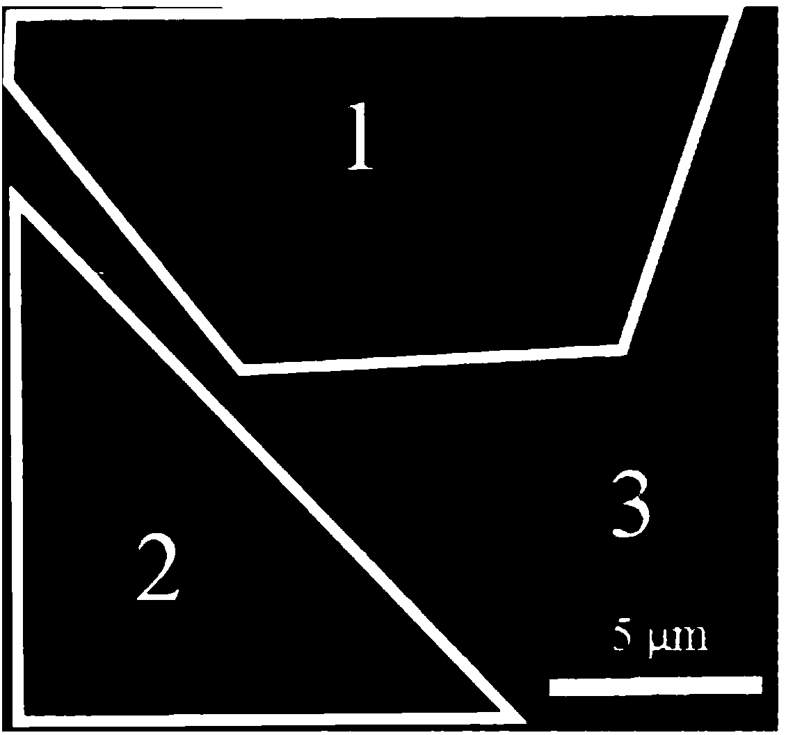
[0044] Using the same method as in Example 1, transfer ReS on heavily doped silicon or silicon dioxide substrates 2 thin slices, and deposited titanium / gold as contact electrodes on both sides of the material by electron beam lithography, and carried out the deposition of nano-gold layer and high-temperature annealing process. The scanning electron microscope image of the prepared sample is shown in image 3 shown. Among them: 1 is ReS 2 Gold on the sheet and surface; 2 is the electrode after annealing;

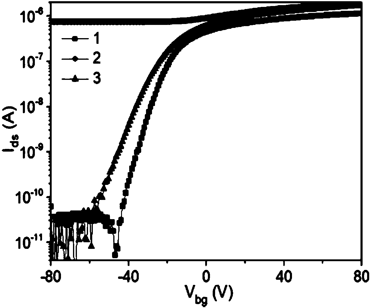
[0045] Electrical tests were performed on the sample, such as Figure 4 As shown in the middle curve 1, the ground state transfer characteristic curve of the device shows strong n-type characteristics, and after the device is exposed to ultraviolet light, its current transfer characteristic curve shows N-type doping characteristics.

[0046] After using a hand-held UV lamp to irradiate the device with ultraviolet light, the transfer characteristic curve is as follows Fig...

Embodiment 3

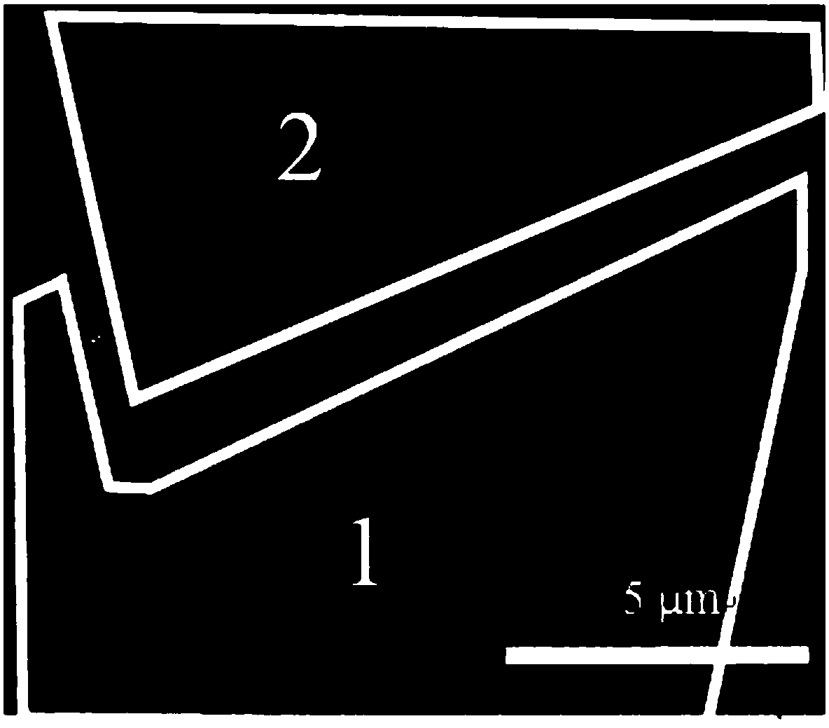
[0048] Using the same method as in Example 1, transfer MoSe on heavily doped silicon or silicon dioxide substrates 2 Thin slices, MoSe2 thin slices, followed by electron beam lithography to deposit titanium / gold on both sides of the material as contact electrodes, and perform nano-gold layer deposition and high-temperature annealing process. The prepared samples are shown in Figure 5 shown.

[0049] Electrical tests were performed on the sample, such as Figure 6 As shown in the middle curve 1, the ground state transfer characteristic curve of the device shows strong N-type characteristics, and after the device is exposed to ultraviolet light, its current transfer characteristic curve shows N-type doping characteristics.

[0050] After using a hand-held UV lamp to irradiate the device with ultraviolet light, the transfer characteristic curve is as follows Figure 6 Shown in curve 2. Its current transfer characteristic curve shows N-type doping characteristics, which is spe...


PUM

PropertyMeasurementUnit
thicknessaaaaaaaaaa
thicknessaaaaaaaaaa

Abstract

The invention discloses a method for performing optical degeneration doping on transition metal sulfide and application of the method. A gold nano layer is deposited on the surface of a two-dimensional material through electron beam evaporation, and a gold nano film with good wettability is formed on the surface of a TMDc material after high-temperature annealing treatment. Under the irradiation of ultraviolet light, electrons of the gold nano layer overflow due to an external photoelectric effect and are injected into the semiconductor layer, and redundant electrons form stable N-type dopingon the semiconductor layer. After the ultraviolet light irradiation is removed, the photon-generated surplus electrons are still retained in the material, so that the doping mode has long-term stability, and meanwhile, the method has universality and can be applied to various N-type TMDc materials. By use of the novel rapid, simple, convenient, universal and stable doping method, a new idea is created for the research of the two-dimensional semiconductor material.

Description

technical field [0001] The invention relates to the technical field of semiconductor material modification, in particular to a method for optically degenerate doping of transition metal sulfides, and in particular to an N-type doping method for two-dimensional semiconductor materials. Background technique [0002] With the development of Moore's Law, silicon-based semiconductors have developed to the limit node. In recent years, semiconducting two-dimensional transition metal dichalcogenides (TMDs) with tunable bandgap have been favored due to their large carrier mobility, high field-effect switching ratio, low subthreshold swing and effective short-channel effect suppression. It is regarded as a substitute for the next generation of silicon-based semiconductors. In order to realize the functions of silicon-based semiconductors, doping TMDs has received extensive attention. Traditional doping methods include ion implantation and in-situ growth atom replacement, but for two...

Claims


Application Information

Patent Timeline
Patent Type & Authority Applications(China)
IPC IPC(8): H01L31/18H01L31/032H01L31/113
CPCH01L31/18H01L31/032H01L31/113Y02P70/50
Inventor 刘晶张荣杰
Owner TIANJIN UNIV
Why Eureka
Try Eureka