Regional layered deposition diffusion process

A layered deposition and diffusion process technology, applied in the direction of climate sustainability, sustainable manufacturing/processing, photovoltaic power generation, etc., can solve the problems of weak regional diffusion controllability, poor blue light response of batteries, and low minority carrier lifetime. Achieve excellent high minority carrier lifetime, reduce recombination, and reduce the concentration of impurity sources

Active Publication Date: 2019-08-23
HENGDIAN GRP DMEGC MAGNETICS CO LTD
View PDF10 Cites 18 Cited by
  • Summary
  • Abstract
  • Description
  • Claims
  • Application Information

AI Technical Summary

Problems solved by technology

[0008] In order to solve the problems of high doping concentration on the surface of the existing PERC+LDSE cells, weak regional diffusion controllability, poor blue light response of the cell, and low minority carrier lifetime, the present invention provides a regional layered deposition and diffusion process. The diffusion process adopts regional layered diffusion control, so that there is a uniform phosphosilicate glass layer on the surface of the silicon wafer, which is conducive to the heavy doping of laser SE, thereby improving the ohmic contact and good contact performance of the cell, and making the emitter region have a Low doping concentration and high-quality PN junction, so that the cell has the characteristics of excellent blue light response and high minority carrier lifetime, and finally improves the conversion efficiency of the cell

Method used


Image

  • Regional layered deposition diffusion process
  • Regional layered deposition diffusion process

Examples


Embodiment 1

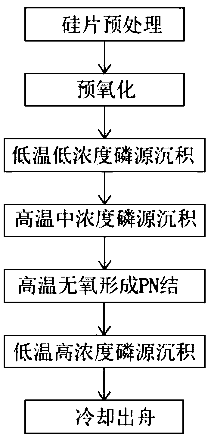
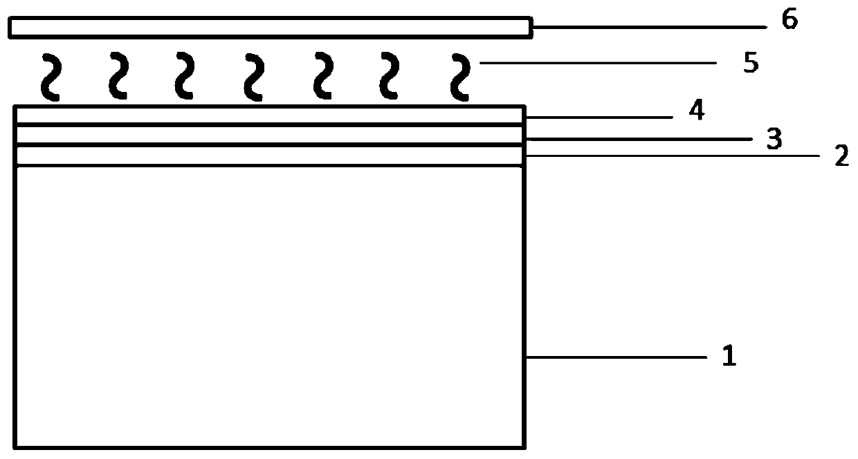
[0034] (1) if figure 1 and figure 2 As shown, silicon wafer pretreatment: clean and texture the P-type original silicon wafer 1, put it into a quartz boat, and push it into the furnace tube of the diffusion furnace;

[0035] (2) Pre-oxidation: raise the temperature of the diffusion furnace to 680°C, inject 3000 sccm of nitrogen and 3000 sccm of oxygen, control the pressure of the furnace tube at 50 mbar, and pre-oxidize the silicon wafer after texturing for 10 minutes to form SiO 2 Layer 2;

[0036] (3) Low temperature and low concentration POCl 3 Deposition: heat up the diffusion furnace to a temperature of 700°C, and inject POCl 3 300sccm, oxygen 700sccm, nitrogen 1000sccm, controlled furnace tube pressure 80mbar, low-temperature and low-concentration phosphorus source deposition on the pre-oxidized silicon wafer for 5min to form low-concentration POCl 3 deposition layer 3;

[0037] (4) Medium concentration POCl in temperature rise 3 Deposition: heat up the diffusion...

Embodiment 2

[0042] (1) if figure 1 and figure 2 As shown, silicon wafer pretreatment: clean and texture the P-type original silicon wafer 1, put it into a quartz boat, and push it into the furnace tube of the diffusion furnace;

[0043] (2) Pre-oxidation: raise the temperature of the diffusion furnace to 700°C, inject 4000 sccm of nitrogen and 4000 sccm of oxygen, control the pressure of the furnace tube to 100 mbar, and pre-oxidize the silicon wafer after texturing for 12 minutes to form SiO 2 Layer 2;

[0044] (3) Low temperature and low concentration POCl 3 Deposition: heat up the diffusion furnace to a temperature of 710°C, and feed POCl 3 250sccm, oxygen 750sccm, nitrogen 1100sccm, controlled furnace tube pressure 100mbar, low-temperature and low-concentration phosphorus source deposition on the pre-oxidized silicon wafer for 4min to form low-concentration POCl 3 deposition layer 3;

[0045] (4) Medium concentration POCl in temperature rise 3 Deposition: heat up the diffusion...

Embodiment 3

[0050] (1) if figure 1 and figure 2 As shown, silicon wafer pretreatment: clean and texture the P-type original silicon wafer 1, put it into a quartz boat, and push it into the furnace tube of the diffusion furnace;

[0051] (2) Pre-oxidation: raise the temperature of the diffusion furnace to 720°C, inject 5000 sccm of nitrogen and 5000 sccm of oxygen, control the pressure of the furnace tube at 150 mbar, and pre-oxidize the silicon wafer after texturing for 15 minutes to form SiO 2 Layer 2;

[0052] (3) Low temperature and low concentration POCl 3 Deposition: maintain the temperature of the diffusion furnace at 720°C, and feed POCl 3 200sccm, oxygen 800sccm, nitrogen 1200sccm, controlled furnace tube pressure 150mbar, low-temperature and low-concentration phosphorus source deposition on the pre-oxidized silicon wafer for 3min to form low-concentration POCl 3 deposition layer 3;

[0053] (4) Medium concentration POCl in temperature rise 3 Deposition: raise the temperat...


PUM


Abstract

The invention relates to the technical field of crystalline silicon solar cells, and provides a regional layered deposition diffusion process in order to solve the problems of over-high surface dopingconcentration, weak regional diffusion controllability, poor cell blue light response and short minority carrier lifetime of an existing PERC+LDSE cell sheet. The process comprises the following steps: (1) pretreatment of a silicon wafer; (2) pre-oxidizing; (3) low-temperature low-concentration phosphorus source deposition; (4) high-temperature medium-concentration phosphorus source deposition; (5) forming of a PN junction; (6) depositing of a low-temperature high-concentration phosphorus source; (7) cooling, pushing of a quartz boat, and taking-out of the silicon wafer. Regional layered diffusion control is adopted in the process, so that a uniform phosphorosilicate glass layer is formed on the surface of a silicon wafer, the laser SE heavy doping is facilitated, and the ohmic contact and good contact performance of a battery piece are improved; and the emitter region has low doping concentration and high-quality PN junctions, so that the battery piece has the characteristics of excellent blue light response and long minority carrier lifetime, and finally, the conversion efficiency of the battery piece is improved.

Description

technical field [0001] The invention relates to the technical field of crystalline silicon solar cells, in particular to a regional layered deposition and diffusion process. Background technique [0002] The cost reduction brought about by the iteration of crystalline silicon solar cell technology has gradually become the main driving force for the development of the industry. In the past two years, the photovoltaic industry cell technology has undergone a transformation from conventional BSF cells → PERC cells → PERC+LDSE cells, of which PERC+LDSE cells The process flow is: texturing→diffusion→laser SE→etching→back passivation→front PECVD→back PECVD→laser slotting→screen printing→sintering→testing. Only one laser SE process is added before the process, and the rest of the process remains unchanged. [0003] The laser SE process uses the phosphosilicate glass layer produced by the diffusion process as the dopant source, and uses the thermal effect of the laser to melt the s...

Claims


Application Information

Patent Timeline
Patent Type & Authority Applications(China)
IPC IPC(8): H01L21/225H01L31/18
CPCH01L21/2256H01L31/1804Y02E10/547Y02P70/50
Inventor 黎剑骑孙涌涛楼城侃王富强
Owner HENGDIAN GRP DMEGC MAGNETICS CO LTD
Why Eureka
Try Eureka