Silicon nanowire chip and mass spectrum detection method based on silicon nanowire chip

A silicon nanowire and mass spectrometry detection technology, applied in the field of new materials and mass spectrometry detection and analysis

Active Publication Date: 2019-09-06
HANGZHOU WELL HEALTHCARE TECH CO LTD
View PDF9 Cites 12 Cited by
  • Summary
  • Abstract
  • Description
  • Claims
  • Application Information

AI Technical Summary

Problems solved by technology

Although a variety of nanomaterials can solve the problem of background interference, their role is limited to replacing o

Method used


Image

  • Silicon nanowire chip and mass spectrum detection method based on silicon nanowire chip
  • Silicon nanowire chip and mass spectrum detection method based on silicon nanowire chip
  • Silicon nanowire chip and mass spectrum detection method based on silicon nanowire chip

Examples


Embodiment Construction

[0098] The present invention will be specifically introduced below in conjunction with the accompanying drawings and specific embodiments.

[0099] A silicon nanowire chip, the manufacturing process is as follows:

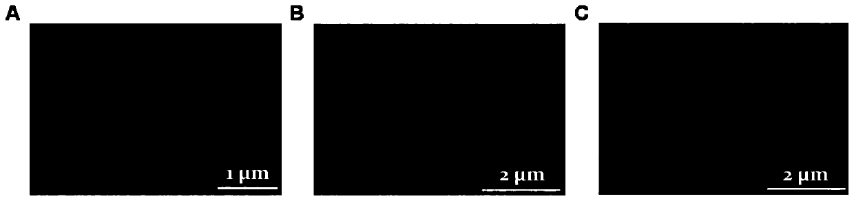
[0100] Step 1, the surface of the single crystal silicon wafer is washed and pretreated, and then subjected to metal-assisted etching and alkali post-etching to obtain a silicon nanowire chip with a cutting edge;

[0101] The steps of surface cleaning and pretreatment of single crystal silicon wafers are as follows: in a clean room, use a laser or a diamond knife to slice a p-type or n-type crystal plane single crystal silicon wafer to obtain a regular rectangular size, The general size is 20mm×20mm; use concentrated sulfuric acid / hydrogen peroxide mixed solution, acetone, ethanol, isopropanol, deionized water, etc. for ultrasonic cleaning to remove organic matter and dust on the surface of the material.

[0102] The metal-assisted etching step of single crystal ...


PUM

PropertyMeasurementUnit
Lengthaaaaaaaaaa

Abstract

The invention discloses a silicon nanowire chip and a mass spectrum detection method and detection method based on the silicon nanowire chip. The mass spectrum detection method comprises the followingsteps: step 1, manufacturing the silicon nanowire chip; carrying out surface washing pretreatment on the monocrystalline silicon wafer, carrying out metal-assisted etching, and carrying out alkali etching to obtain a silicon nanowire chip with a tip; carrying out surface chemical or nano material modification on the silicon nanowire chip; step 2, evaluating the mass spectrum performance of the silicon nanowire chip; step 3, carrying out top contact sampling and in-situ ionization mass spectrometry detection. According to the method, the nanostructure characteristic and the semiconductor characteristic of the silicon nanowire chip are fully utilized, contact type extraction transfer printing and matrix-free mass spectrometry detection are integrated, and the collection, pretreatment and detection processes of complex samples are greatly simplified; the silicon nanowire chip manufactured by the method has adsorption and extraction functions and a mass spectrum detection function at thesame time, and in-situ information of a sample with spatial heterogeneity can be reserved.

Description

technical field [0001] The invention belongs to the technical field of new materials and mass spectrometry detection and analysis methods, and in particular relates to a silicon nanowire chip and a mass spectrometry detection method based on the silicon nanowire chip. Background technique [0002] The collection, pretreatment and detection of biological samples are three important links in the field of analytical technology. Compared with conventional analysis methods, mass spectrometry has the characteristics of high accuracy, high sensitivity, and high content, and is especially suitable for qualitative and quantitative analysis of trace analytes in complex samples and parallel analysis of multiple analytes. play an important role in clinical diagnosis. Among them, the method based on matrix-assisted laser desorption / ionization (MALDI) provides a good platform for the rapid detection of complex samples due to its high speed, high throughput, and strong anti-pollution char...

Claims


Application Information

Patent Timeline
IPC IPC(8): B81B1/00B81B7/04B81C1/00G01N27/62
CPCB81B7/04B81B1/00B81C1/00031B81C1/00111B81C1/00206G01N27/62B81B2203/0361B81B2207/056H01J49/0418G01N27/68B81C2201/0133G01N27/623G01N27/64
Inventor 邬建敏陈晓明
Owner HANGZHOU WELL HEALTHCARE TECH CO LTD
Why Eureka
Try Eureka