Silicon carbide MOSFET device with T-type masking layer structure

A silicon carbide and masking layer technology, applied in the field of microelectronics, can solve problems affecting the forward blocking characteristics of devices, device breakdown, gate dielectric layer breakdown, etc., to reduce switching power consumption, reduce gate-drain capacitance, Mitigate the effect of capacitive coupling

Inactive Publication Date: 2019-09-06
XIDIAN UNIV
View PDF3 Cites 2 Cited by
  • Summary
  • Abstract
  • Description
  • Claims
  • Application Information

AI Technical Summary

Problems solved by technology

[0004] At present, in the traditional groove gate structure MOSFET device, it has been able to achieve a higher withstand voltage level by design, but in practical applications, the electric field concentration at the corner of the gate oxide layer in the groove gate structure MOSFET device leads to the shock of the gate dielectric layer. breakdown, causing the device to break down below the rated breakdown voltage, seriously affecting the forward blocking characteristics of the device

Method used


Image

  • Silicon carbide MOSFET device with T-type masking layer structure
  • Silicon carbide MOSFET device with T-type masking layer structure
  • Silicon carbide MOSFET device with T-type masking layer structure

Examples


Embodiment Construction

[0042] In order to further explain the technical means and effects of the present invention to achieve the intended purpose of the invention, a silicon carbide MOSFET device with a T-shaped masking layer structure proposed according to the present invention will be described in detail below in conjunction with the accompanying drawings and specific implementation methods.

[0043] The aforementioned and other technical contents, features and effects of the present invention can be clearly presented in the following detailed description of specific implementations with accompanying drawings. Through the description of specific embodiments, the technical means and effects of the present invention to achieve the intended purpose can be understood more deeply and specifically, but the accompanying drawings are only for reference and description, and are not used to explain the technical aspects of the present invention. program is limited.

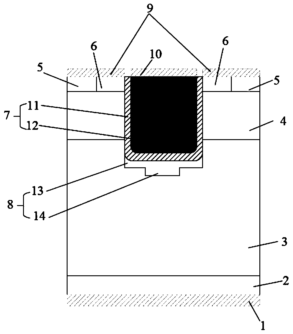
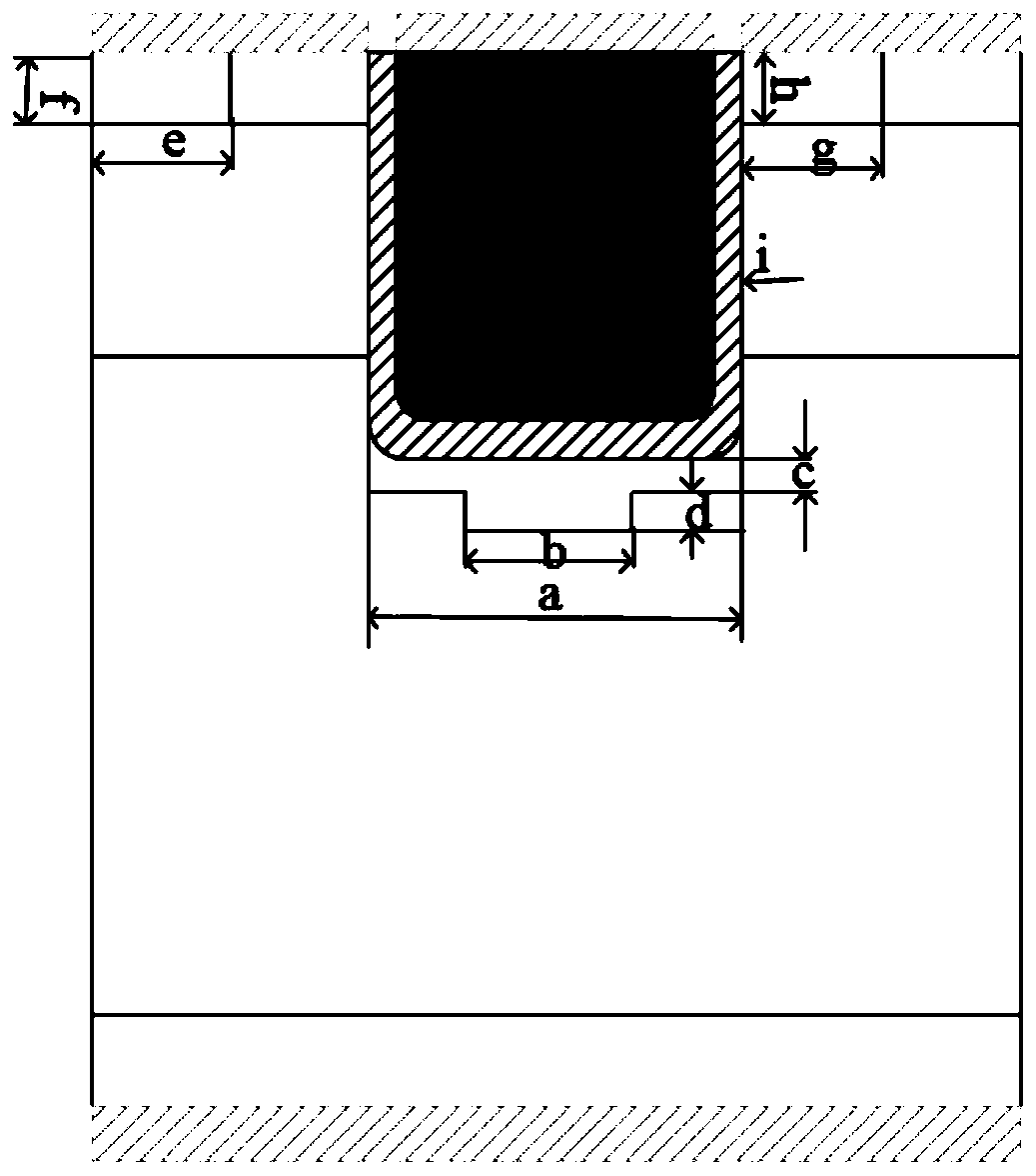
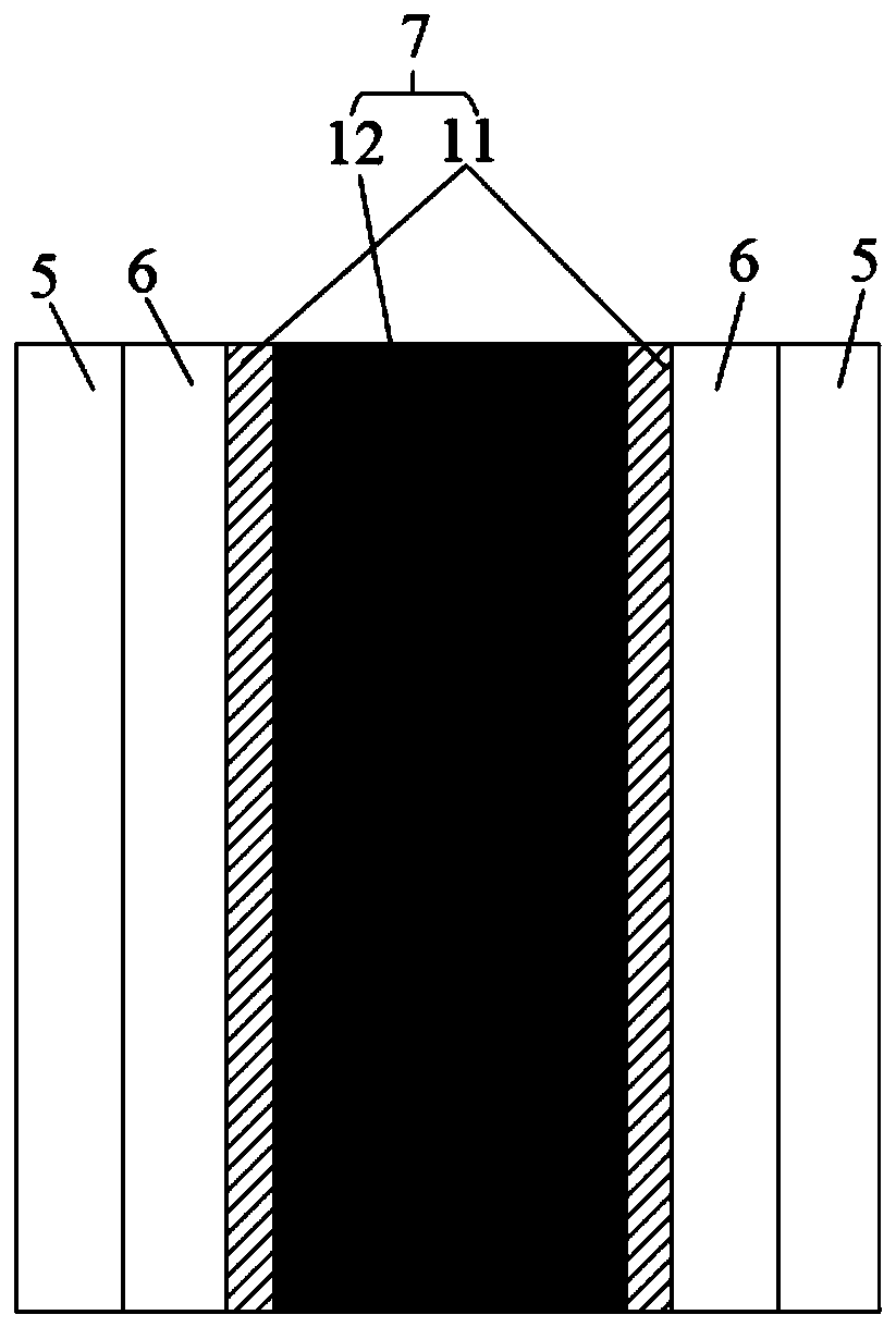
[0044] See figure 1 , figure 1 It is ...


PUM


Abstract

The invention relates to a silicon carbide MOSFET device with a T-type masking layer structure. The silicon carbide MOSFET device comprises a drain electrode, an N-type doped substrate layer, an N-type drift region and a P-type base region which are sequentially arranged from bottom to top; P-type source regions and N-type source regions are arranged on the P-type base region; a groove gate structure is arranged in the P-type base region; the bottom of the groove gate structure extends into the interior of the N-type drift region, and the top of the groove gate structure extends out of the upper surface of the P-type base region; the T-shaped masking layer structure is arranged below the groove gate structure, and the upper surface of the T-shaped masking layer structure is in contact withthe lower surface of the groove gate structure; source electrodes are arranged on the P-type source regions and the N-type source regions; and a gate electrode is arranged on the groove gate structure. According to the silicon carbide MOSFET device, the T-shaped masking layer structure is added at the bottom of the groove gate structure, so that the breakdown voltage of the device is improved, the switching speed of the device is increased, and meanwhile, the switching power consumption of the device is reduced.

Description

technical field [0001] The invention belongs to the technical field of microelectronics, and in particular relates to a silicon carbide MOSFET device with a T-shaped masking layer structure. Background technique [0002] Silicon carbide, a wide bandgap semiconductor material, has excellent physical and chemical properties such as large bandgap width, high critical breakdown electric field, high thermal conductivity and high electron saturation drift velocity, and is suitable for high temperature, high pressure, high power and radiation resistance semiconductor devices. In the field of power electronics, power Metal-Oxide-Semiconductor-Field-Effect-Transistor (MOSFET, Metal-Oxide-Semiconductor-Field-Effect-Transistor) has been widely introduced, and it has the characteristics of simple gate drive and short switching time. [0003] Trench gate structure MOSFET is a new high-efficiency power switching device developed after MOSFET. It adopts trench gate structure field effect ...

Claims


Application Information

Patent Timeline
Patent Type & Authority Applications(China)
IPC IPC(8): H01L29/06H01L29/78
CPCH01L29/0623H01L29/7827
Inventor 宋庆文张玉明白瑞杰汤晓燕张艺蒙王悦湖
Owner XIDIAN UNIV
Why Eureka
Try Eureka