A kind of high temperature resistant PCB board and its production process

A technology of PCB board and high temperature resistance, applied in the field of PCB board manufacturing, can solve the problem that the heat resistance performance of the PCB board does not meet the requirements for use, achieve good thermal conductivity and heat dissipation, improve thermal conductivity, and facilitate the effect of phonon propagation.

Active Publication Date: 2021-11-19
深圳市福源晖集成电子有限公司
View PDF1 Cites 0 Cited by
  • Summary
  • Abstract
  • Description
  • Claims
  • Application Information

AI Technical Summary

Problems solved by technology

However, since the PCB board prepared in this application is only processed with solder paste on the surface, the PCB board cannot meet the requirements for use in terms of heat resistance.

Method used


Image

  • A kind of high temperature resistant PCB board and its production process
  • A kind of high temperature resistant PCB board and its production process

Examples


Embodiment 1

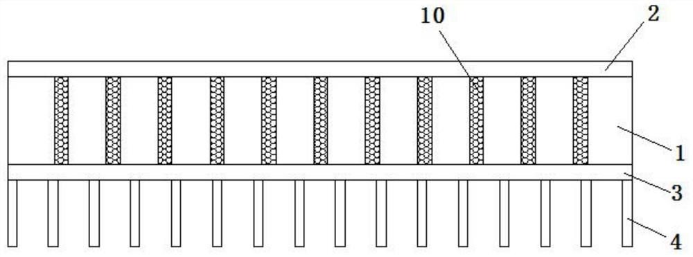
[0066] Substrate 11 is made by following method:

[0067] S1. Weigh phosphorus-containing flame-retardant epoxy resin, add it to a three-necked bottle, heat to 35°C, add epoxy resin, and mix at 300r / min for 30min; the mass ratio of phosphorus-containing flame-retardant epoxy resin to epoxy resin is 1 :1;

[0068] S2. Add acetone and dimethylformamide, mix at 300r / min for 30min, add melamine, mix for 15min, then add the mixture of boron nitride and silicon carbide, and stir at a high speed for 60min at a speed of 3000r / min to obtain a modified epoxy resin;

[0069] Wherein, the addition amount of the mixture of boron nitride and silicon carbide is 16% of the mass of the resin mixture, and the mass ratio of BN and SiC is 9:1;

[0070] S3. Put the modified epoxy resin into a mold and cold press it for 10 minutes to form it, then transfer it to an oven for drying at 160° C. for 50 minutes, and then transfer it to a hot press machine for hot pressing at 160° C. for 55 minutes unt...

Embodiment 2

[0072] Substrate 11 is made by following method:

[0073] S1. Weigh phosphorus-containing flame-retardant epoxy resin, add it to a three-neck bottle, heat to 40°C, add epoxy resin, and mix at 300r / min for 30min; the mass ratio of phosphorus-containing flame-retardant epoxy resin to epoxy resin is 1 :1.2;

[0074] S2. Add acetone and dimethylformamide, mix at 300r / min for 30min, add melamine, mix for 15min, then add the mixture of boron nitride and silicon carbide, and stir at a high speed for 60min at a speed of 3000r / min to obtain a modified epoxy resin;

[0075] Wherein, the addition amount of the mixture of boron nitride and silicon carbide is 18% of the mass of the resin mixture, and the mass ratio of BN and SiC is 9:1;

[0076] S3. Put the modified epoxy resin into a mold and cold press it for 10 minutes to form it, then transfer it to an oven for drying at 160°C for 60 minutes, and then transfer it to a hot press machine for hot pressing at 160°C for 65 minutes until i...

Embodiment 3

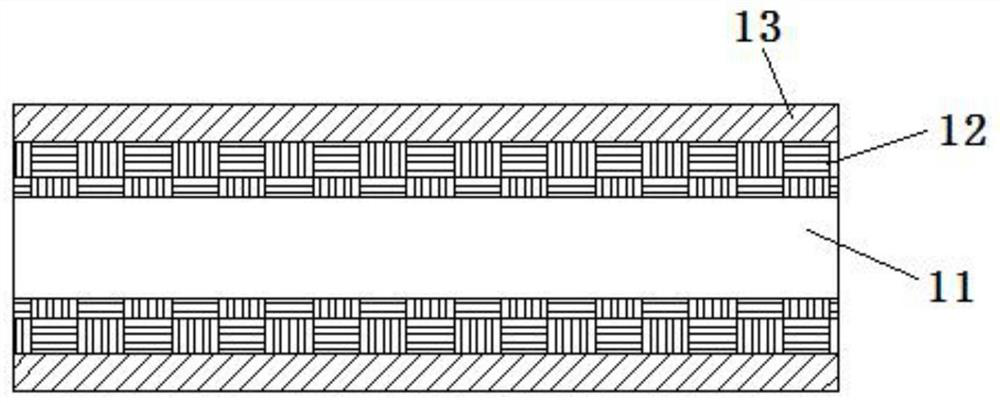
[0084] The potting glue is prepared by the following method:

[0085] (1) Weigh 100g of methylphenyl silicone resin and 24g of butyl acetate and mix and disperse for 30min at a speed of 2000r / min, add 1.6g of methyltrimethoxysilane and 2.4g of phenyltrimethoxysilane, and after adding Continue to disperse for 30-40 minutes;

[0086] (2) Add 1.6g of butyl titanate and 0.3g of γ-(2,3-glycidoxy)propyltrimethoxysilane, increase the rotation speed to 3000r / min, and stir at high speed for 25min;

[0087](3) Finally, 80 g of n-octane was added, stirred at 2000 r / min for 30 min, and the potting glue was prepared.


PUM

PropertyMeasurementUnit
thicknessaaaaaaaaaa
thicknessaaaaaaaaaa
thicknessaaaaaaaaaa

Abstract

The invention discloses a high-temperature-resistant PCB board, which includes a PCB original board, one side of the PCB original board is coated with potting glue to form a potting glue layer, and the other side surface is fixed with heat dissipation fins through a heat-conducting silicone grease layer. The surface is provided with evenly distributed thermal vias along the thickness direction, the original PCB includes a base material, and copper-clad laminates are fixed on both sides of the base material through prepregs; the invention also discloses a manufacturing process of the PCB board. In the present invention, a modified epoxy resin is used as the base material of the PCB board, and a tight heat conduction network is formed in the base material. By opening thermal vias and dissipating fins on the original PCB, the heat generated by the power device passes through the device shell and The potting adhesive layer reaches the copper-clad board on the top of the PCB original board, conducts heat to the copper-clad board at the bottom of the board through the thermal via, and then transfers the heat to the base of the cooling fins through the original board, and then transfers the heat to the surrounding environment through the cooling fins to achieve good The effect of heat conduction and heat dissipation improves the high temperature resistance of the PCB board from multiple aspects such as the PCB board body and surface.

Description

technical field [0001] The invention belongs to the technical field of PCB board manufacturing, and in particular relates to a high-temperature-resistant PCB board and a manufacturing process thereof. Background technique [0002] Printed Circuit Board (PCB) is the basis of almost any electronic product and appears in almost every electronic device. Generally speaking, if there are electronic components in a certain device, they are also integrated in the size vary on the PCB. In addition to fixing various components, the main function of PCB is to provide connection circuits between various components. As electronic equipment becomes more and more complex, more and more components are required, and the lines and components on the surface of the PCB are becoming more and more dense. Due to the high density, multi-function, high power of electronic products and the rapid development of microelectronics integration technology, the power density and calorific value of power e...

Claims


Application Information

Patent Timeline
Patent Type & Authority Patents(China)
IPC IPC(8): H05K1/02H05K3/00
CPCH05K1/021H05K3/0058H05K2201/066
Inventor 许相会
Owner 深圳市福源晖集成电子有限公司
Why Eureka
Try Eureka