Capacitive pressure sensor and manufacturing method thereof

A pressure sensor, capacitive technology, used in fluid pressure measurement using capacitance changes, piezoelectric/electrostrictive/magnetostrictive devices, televisions, etc. Large-scale pressure monitoring requirements, difficult process preparation and other problems, to achieve the effect of improving the linear range, high yield, and large linear range

Active Publication Date: 2019-11-29
XIDIAN UNIV
View PDF8 Cites 3 Cited by
  • Summary
  • Abstract
  • Description
  • Claims
  • Application Information

AI Technical Summary

Problems solved by technology

In 2001, Jiao Yuzhong and others proposed a capacitive pressure sensor with a double-thin film structure, which expanded the linear range of the sensor, but the sensitivity was reduced. See Analysis and Design of Contact Capacitive Pressure Sensor, Jiao Yuzhong, Xiamen University Master Thesis , 2001
However, the invention improves the performance of the sensor by introducing a comb-toothed electrode structure, and the process is difficult to prepare
In 2017, Myong-Chol Kang et al. proposed to improve the shape of the bottom electrode in a capacitive pressure sensor, which expanded the linear range of the sensor, but resulted in a decrease in sensitivity
Therefore, it is difficult to improve the linear pressure range and sensitivity of contact capacitive pressure sensors at the same time, and the linear pressure range is usually small, which cannot meet the monitoring needs of large-scale pressure in many fields such as automotive systems and aerospace.

Method used


Image

  • Capacitive pressure sensor and manufacturing method thereof
  • Capacitive pressure sensor and manufacturing method thereof
  • Capacitive pressure sensor and manufacturing method thereof

Examples


Embodiment 1

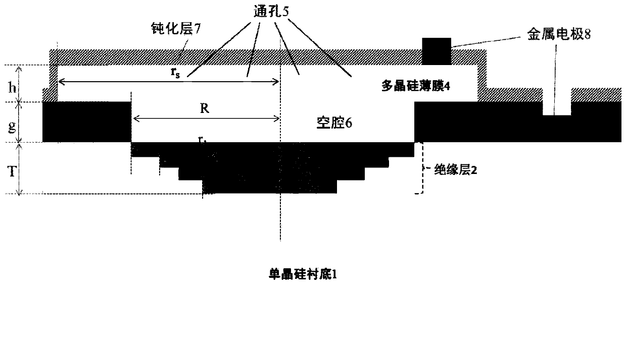
[0050] Example 1: Making the insulating layer as SiO 2 , the isolation layer is SiN, the passivation layer is SiN, and the number of insulating layers is N=2 capacitive pressure sensors.

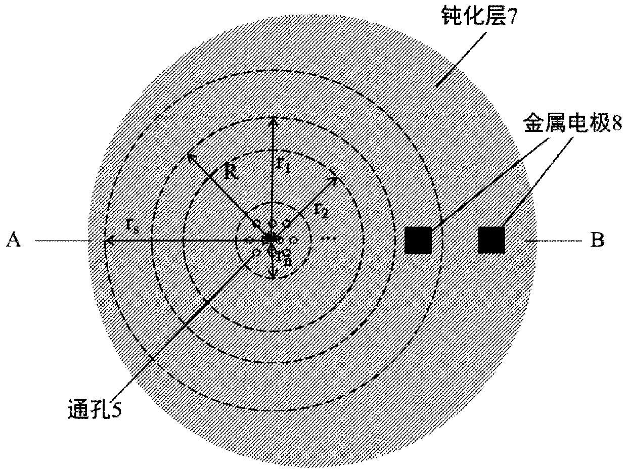
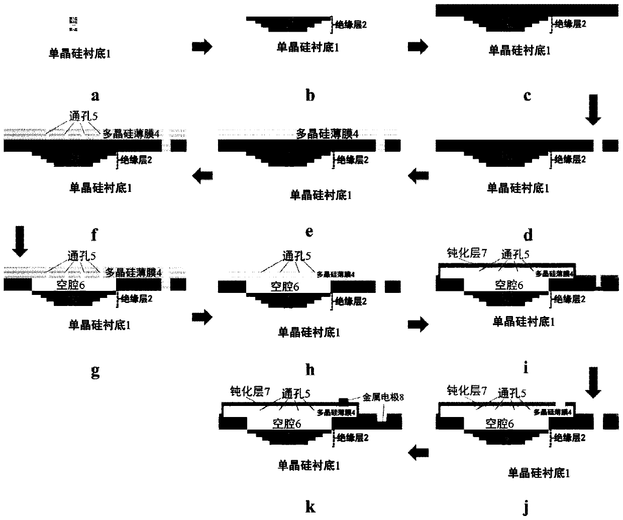
[0051] Step 1, etch the single crystal silicon in the region of the two insulating layers on the single crystal silicon substrate, such as image 3 a.

[0052] 1a) Make a mask on a single crystal silicon substrate, using reactive ion etching technology, that is, on CF 4 Under the process conditions of flow rate of 15sccm, pressure of 10mT and power of 80W, etching thickness t is 125nm, radius r 1 is 100μm of the first layer of insulating layer area;

[0053] 1b) Make a secondary mask on a single crystal silicon substrate, using the same reactive ion etching process conditions as 1a), the etching thickness t is 125nm, the radius r 2 The second insulating layer region is 39 μm.

[0054] Step 2, depositing insulating layer dielectric SiO in the region of the N-layer insulating layer etched...

Embodiment 2

[0074] Example 2: Making the insulating layer as SiO 2 , the isolation layer is SiN, and the passivation layer is Al 2 O 3 , a capacitive pressure sensor with N=4 insulating layers.

[0075] Step 1, etch the single crystal silicon in the area of ​​4 insulating layers on the single crystal silicon substrate, such as image 3 a.

[0076] 1.1) Make a mask on the single crystal silicon substrate, use reactive ion etching technology to etch the first layer of insulating layer region, the thickness t of the first layer of insulating layer region is 0.1μm, the radius r 1 is 250μm;

[0077] 1.2) Make a secondary mask on the single crystal silicon substrate, use reactive ion etching technology to etch the second insulating layer region, the thickness t of the second insulating layer region is 0.1 μm, and the radius r 2 is 123 μm;

[0078] 1.3) Make three masks on the single crystal silicon substrate, use reactive ion etching technology to etch the third insulating layer region, t...

Embodiment 3

[0102] Example 3: Making the insulating layer as SiO 2 , the isolation layer is SiN, and the passivation layer is HfO 2 , a capacitive pressure sensor with N=5 insulating layers.

[0103] Step A, etching the single crystal silicon in the area of ​​5 layers of insulating layers on the single crystal silicon substrate, such as image 3 a.

[0104] First, make a mask on the single crystal silicon substrate, and use reactive ion etching technology to etch the first insulating layer region. The thickness t of the first insulating layer region is 0.16μm, and the radius r 1 is 500μm; then a secondary mask is made on the single crystal silicon substrate, using reactive ion etching technology, the etching thickness t is 0.16μm, the radius r 2 The second insulating layer area is 260 μm, and then three masks are made on the single crystal silicon substrate, using reactive ion etching technology, the etching thickness t is 0.16 μm, the radius r 3 It is the third insulating layer area ...


PUM

PropertyMeasurementUnit
thicknessaaaaaaaaaa
radiusaaaaaaaaaa
heightaaaaaaaaaa

Abstract

The invention discloses a capacitive pressure sensor and a manufacturing method thereof. The problem that an existing pressure sensor is small in linear range is mainly solved. The sensor comprises amonocrystalline silicon substrate (1), an insulating layer (2), an isolating layer (3) and a polycrystalline silicon film (4) from bottom to top. The insulating layer (2) is composed of N stacked circular steps, wherein the radius of each stacked circular step is gradually reduced from top to bottom. Wherein N is not less than 2, and the thicknesses of the circular steps are the same; the polycrystalline silicon film (4) has different radii, a through hole (5) for corroding the isolation layer (3) is etched on the polycrystalline silicon film (4), the isolation layer (3) forms a cavity (6) through corrosion, metal electrodes (8) are deposited on the polycrystalline silicon film (4) and the monocrystalline silicon substrate (1), and passivation layers (7) cover other surfaces of the isolation layer, the through hole and the polycrystalline silicon film except the metal electrodes. The invention has the advantages of large linear range, simple process and high yield, and can be used formeasuring large-range pressure in the fields of automobile systems and industry.

Description

technical field [0001] The invention belongs to the technical field of electronic devices, and in particular relates to a capacitive pressure sensor, which can be used for measuring a wide range of pressure in automotive systems and industrial fields. [0002] technical background [0003] The MEMS pressure sensor is the core component of the pressure monitoring system. Its function is to convert the external pressure into a capacitance signal to be recognized and processed by the system. MEMS pressure sensors have the characteristics of high sensitivity, low power consumption, small size and easy integration, and have important and extensive applications in the fields of intelligent electronics, biomedical, aerospace and automotive systems. Therefore, many scientific research institutions and colleges and universities have invested a lot of money and manpower to study MEMS pressure sensors. [0004] The working modes of MEMS pressure sensors are mainly piezoresistive, capac...

Claims


Application Information

Patent Timeline
Patent Type & Authority Applications(China)
IPC IPC(8): B81B7/02B81C1/00G01L1/14G01L9/12
CPCB81B7/02B81C1/00349B81C1/00531G01L1/148G01L9/12B81B2201/0264B81C2201/0132
Inventor 杨翠史芝纲毛维
Owner XIDIAN UNIV
Why Eureka
Try Eureka