Flexible nitride thin film solar cell and manufacturing method thereof
A solar cell and manufacturing method technology, applied in circuits, photovoltaic power generation, electrical components, etc., can solve the problems of heavy device structure, product damage, and complicated processes, and achieve high energy conversion efficiency, light weight, and high absorption coefficient. Effect
- Summary
- Abstract
- Description
- Claims
- Application Information
AI Technical Summary
Problems solved by technology
Method used
Image
Examples
Embodiment 1
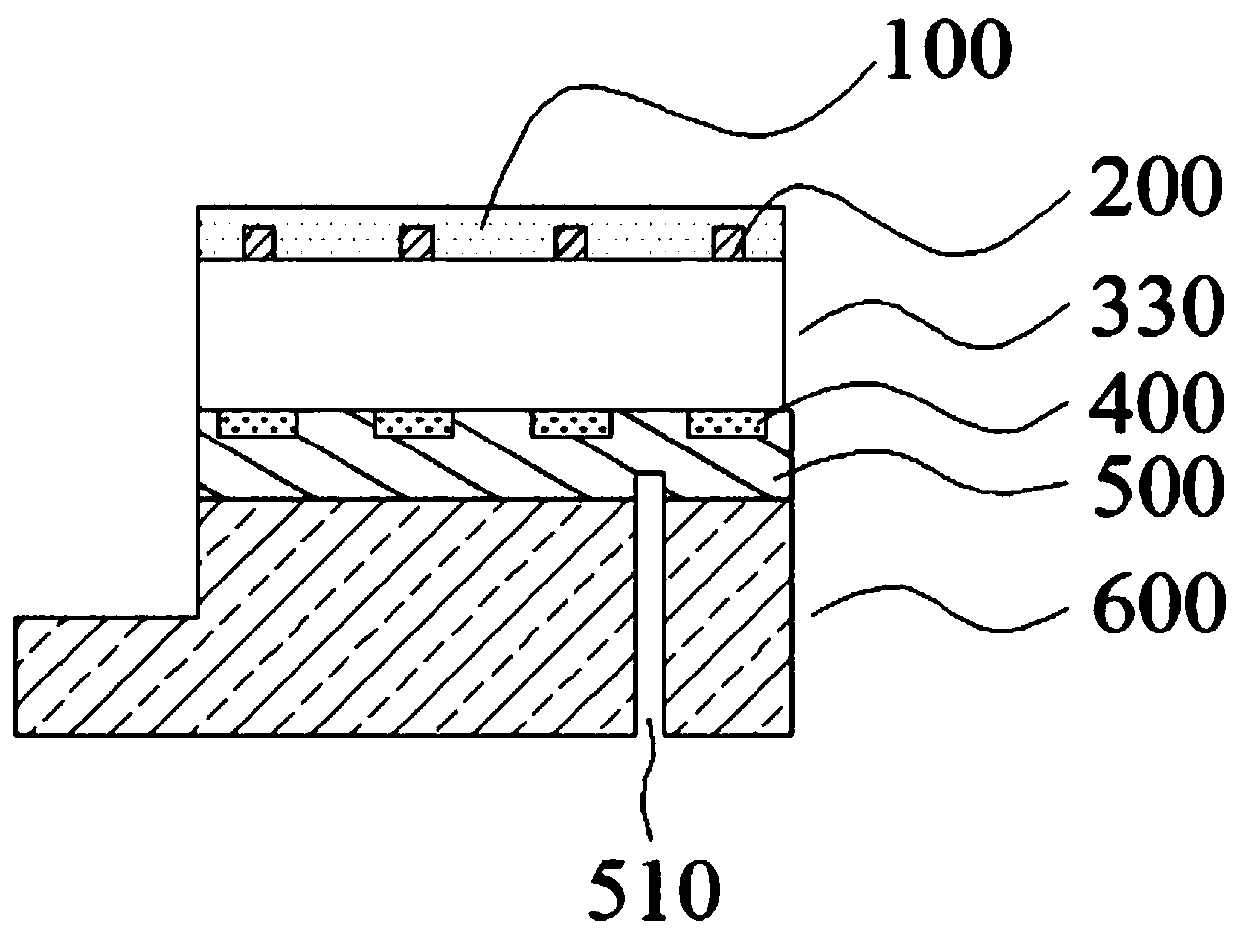
[0094] The flexible nitride thin film solar cell described in the first embodiment is composed of a support substrate 600, a back electrode 500, a dielectric reflection layer 400, a nitride epitaxial layer 330, a front electrode 200 and an antireflection layer 100 from bottom to top, And the via structure 510 penetrates through the supporting substrate and reaches the inside of the back electrode 500 . Wherein, the supporting substrate 600 is made of polyethylene terephthalate (PET); the dielectric reflection layer 400 is made of insulating ink.
[0095] Further, the back electrode 500 is an ohmic contact electrode composed of multi-layer metal thin film functional layers, and according to the direction from the nitride epitaxial layer 330 to the support substrate 600, it includes: an adhesion layer 520, an electrode reflective layer 530, a first preliminary Stress layer 540 , barrier layer 550 and conductive layer 560 . Wherein, the adhesive layer 520 is made of metal Ni thi...
Embodiment 2
[0101] The second embodiment discloses a method for making the flexible nitride thin film solar cell as described in the first embodiment, which further refines the above-mentioned preparation method into the following steps:
[0102]Step 1, such as Figure 4 As shown, a graphene sacrificial layer 320 is prepared on a 4H-SiC substrate wafer 310;
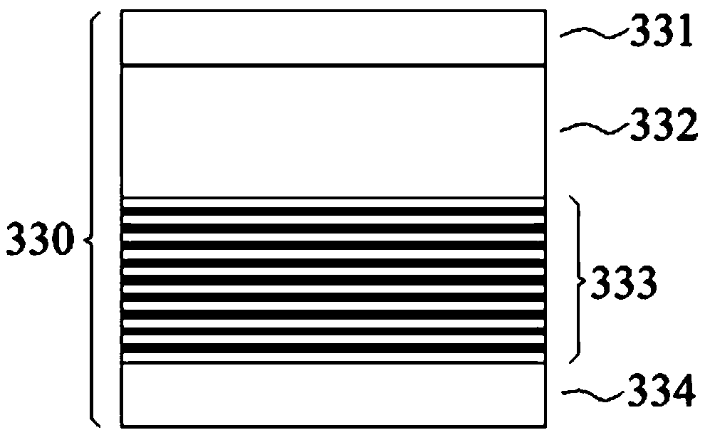
[0103] Step 2, such as Figure 5 As shown, on the sacrificial layer 320, a nitride epitaxial layer 330 having a thin-film solar cell structure as described in Embodiment 1 or Embodiment 2 is grown;
[0104] Step 3, such as Figure 6 As shown, a dielectric reflective layer 400 is formed on the nitride epitaxial layer 330;
[0105] Step 4, such as Figure 7 As shown, the back electrode 500 is made on the dielectric reflective layer 400 and the nitride epitaxial layer 330, and at the same time, the back electrode 500 is used as the first prestressed layer;
[0106] Step 5, such as Figure 8 As shown, the second prestressed layer 7...
Embodiment 3
[0121] Embodiment 3 discloses another method for manufacturing the flexible nitride thin-film solar cell as described in Embodiment 1. It should be noted that, in the manufacturing method described in the third embodiment, the same parts as the method described in the second embodiment will not be repeated, and only the different parts will be described in detail.
[0122] Specifically, the method further refines the preparation method into the following steps:
[0123] Step 1, such as Figure 4 As shown, a graphene sacrificial layer 320 is prepared on a 6H-SiC substrate wafer 310;
[0124] Step 2, such as Figure 5 As shown, on the sacrificial layer 320, a nitride epitaxial layer 330 having a thin-film solar cell structure as described in Embodiment 1 or Embodiment 2 is grown;
[0125] Step 3, such as Figure 6 As shown, a dielectric reflective layer 400 is formed on the nitride epitaxial layer 330;
[0126] Step 4, such as Figure 7 As shown, the back electrode 500 is ...
PUM
| Property | Measurement | Unit |
|---|---|---|
| Thickness | aaaaa | aaaaa |
Abstract
Description
Claims
Application Information


