Preparation method of surface plasmon metamaterial

A surface plasmon and metamaterial technology, which is applied in the fields of nanophotonics and nanofabrication, can solve the problems of low yield, high cost, and few types of processing structures, and achieves huge application potential, simple process method, and enhanced optical absorption. Effect

Active Publication Date: 2019-12-31
PEKING UNIV
View PDF4 Cites 2 Cited by
  • Summary
  • Abstract
  • Description
  • Claims
  • Application Information

AI Technical Summary

Problems solved by technology

The currently used process methods are usually relatively expensive, have low yield, c

Method used


Image

  • Preparation method of surface plasmon metamaterial
  • Preparation method of surface plasmon metamaterial
  • Preparation method of surface plasmon metamaterial

Examples


Embodiment 1

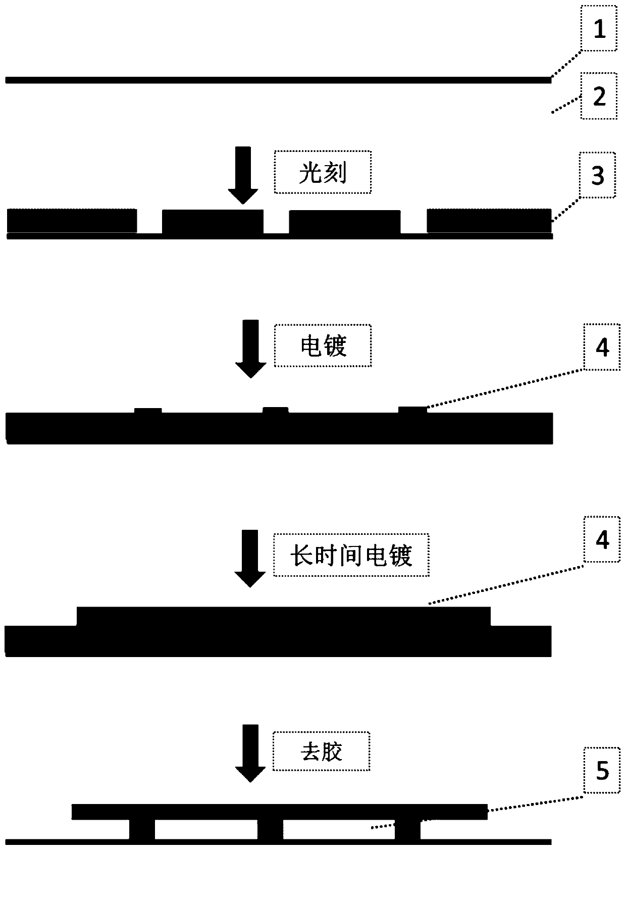
[0027] (1) The substrate material is glass;

[0028] (2) On the glass substrate, the metal film deposited by electron beam evaporation coating is: 3 nanometers of titanium and 5 nanometers of gold;

[0029] (3) Use electron beam lithography to carry out photolithography to form patterning on the metal film, specifically: first spin 120 nanometers of thickness to coat photoresist PMMA, and prepare predetermined pattern by exposure and development;

[0030] (4) Electroplating filling photolithography pattern: electroplating by square wave pulse method, voltage is 10V, duty cycle is 20%, current is 0.001A, time is 10 minutes;

[0031] (5) electroplating growth gold film: adopt square wave pulse method electroplating, voltage is 10V, duty ratio is 80%, electric current is 0.01A, time is 5 minutes;

[0032] (6) Soak the substrate in an acetone solution to remove residual photoresist; form a cavity-coupled resonant surface plasmon metamaterial with a metal-air dielectric layer-meta...

Embodiment 2

[0034] (1) The substrate material is glass;

[0035] (2) On the glass substrate, the metal film deposited by electron beam evaporation coating is: 3 nanometers of chromium and 5 nanometers of silver;

[0036] (3) Use electron beam lithography to carry out photolithography to form patterning on the metal film, specifically: first spin 120 nanometers of thickness to coat photoresist PMMA, and prepare predetermined pattern by exposure and development;

[0037] (4) Electroplating filling photolithographic pattern: electroplating by square wave pulse method, voltage is 20V, duty cycle is 50%, current is 0.001A, time is 5 minutes;

[0038] (5) electroplating growth gold film: adopt square wave pulse method electroplating, voltage is 20V, duty cycle is 50%, electric current is 0.001A, time is 10 minutes;

[0039] (6) Soak the substrate in an acetone solution to remove residual photoresist; form a cavity-coupled resonant surface plasmon metamaterial with a metal-air dielectric layer-...

Embodiment 3

[0041] (1) The substrate material is glass;

[0042] (2) Depositing an indium tin oxide thin film on a glass substrate with an evaporation coating, the thickness is between 5-20 nanometers;

[0043] (3) Use a UV lithography machine to perform photolithography to form a pattern, specifically: first spin-coat a 150-nanometer UV photoresist, and prepare a predetermined pattern through exposure and development;

[0044] (4) Electroplating and filling photolithographic patterns: square wave pulse method is used for electroplating, the voltage is 10V, the duty cycle is 20%, the current is 0.01A, and the time is 15 minutes;

[0045] (5) Gold film grown by electroplating: the voltage is 80V, the duty cycle is 20%, the current is 0.01A, and the time is 45 minutes;

[0046] (6) The substrate is immersed in an acetone solution to remove residual photoresist; a cavity-coupled resonant surface plasmon metamaterial with a metal-air dielectric layer-metal structure is formed.


PUM

PropertyMeasurementUnit
Thicknessaaaaaaaaaa

Abstract

The invention provides a preparation method of a surface plasmon metamaterial, and belongs to the technical field of nanophotonics and nanofabrication. According to the preparation method, the thickness of a spin-coated photoresist is controlled through an electroplating process to realize control over the thickness of an intermediate layer in metal-medium-metal, and different medium thicknesses can serve as an optical cavity and can be coupled with surface plasmons to realize different optical responses; and meanwhile, optical absorption is enhanced by means of the ohmic loss of metal, almost-perfect optical absorption (the absorption rate is close to 100%) and high-quality factor optical cavities are realized by means of the electromagnetic energy localization effect of the surface plasmons. The technical method is simple, stable and cheap and can realize large-area processing.

Description

technical field [0001] The invention relates to the technical fields of nanophotonics and nanoprocessing, in particular to a method for preparing a surface plasmon metamaterial. Background technique [0002] Surface plasmons are mainly based on the interaction process of electromagnetic radiation and conduction electrons in metal interfaces or subwavelength metal structures. This interaction will lead to optical near-field enhancement and optical nonlinear effects in subwavelength dimensions. Arranging this subwavelength structure into an array according to certain rules can have special electromagnetic properties that are not found in natural materials, that is, surface plasmon metamaterials. The special electromagnetic properties of metamaterials mainly depend on the shape, size, direction and arrangement of subwavelength unit structures. With the continuous development of micro- and nano-processing technology, people can use deep ultraviolet lithography, electron beam ex...

Claims


Application Information

Patent Timeline
IPC IPC(8): C25D5/18C25D5/02C25D5/48C23C14/30C23C14/18C23C14/58C23C14/24C23C14/08
CPCC23C14/086C23C14/18C23C14/24C23C14/30C23C14/5873C25D5/02C25D5/18C25D5/48
Inventor 吴文刚朱佳黄允
Owner PEKING UNIV
Why Eureka
Try Eureka