Grid-line-free and undoped-contact based monocrystalline silicon heterojunction solar cell

A technology for solar cells and monocrystalline silicon, applied in the field of solar photovoltaic, can solve the problems of complex process, limit battery open-circuit voltage and short-circuit current, and high cost, and achieve the effects of simple structure design, simple preparation process and low cost

Pending Publication Date: 2019-12-31
ZHEJIANG UNIV
View PDF0 Cites 6 Cited by
  • Summary
  • Abstract
  • Description
  • Claims
  • Application Information

AI Technical Summary

Problems solved by technology

These doped contact technologies have many disadvantages: From a physical perspective, heavy doping will inevitably lead to unfavorable factors such as Auger recombination, narrowing of the forbidden band, body/surface recombination, and free carrier absorption, which greatly limit the open circuit voltage of the battery. and short-circuit current; from a technical ...

Method used


Image

  • Grid-line-free and undoped-contact based monocrystalline silicon heterojunction solar cell
  • Grid-line-free and undoped-contact based monocrystalline silicon heterojunction solar cell

Examples


Embodiment 1

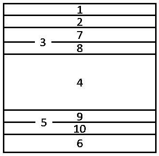
[0034]The anti-reflection film 1 is set to be molybdenum oxide with a thickness of 50 nm; the ultra-thin metal film 2 is an alloy film mixed with aluminum / silver in a ratio of 1:10, and the thickness is 5 nm; the hole selective contact 3 includes a hole selective film 7 and the first passivation film 8 are respectively 10 nm thick molybdenum oxide and 1 nm thick silicon oxide; the thickness of single crystal silicon 4 is 10 μm; the electron selective contact 5 includes the second passivation film 9 and the electron selective The permanent thin film 10 is respectively 1 nm thick silicon oxide and 1 nm thick lithium fluoride; the back electrode 6 is made of aluminum with a thickness of 100 nm.

[0035] On the basis of cleaning the single crystal silicon 4, silicon oxide can be deposited as the first passivation film 8 and the second passivation film 9 by using the atomic layer deposition method, and then by thermal evaporation method, on one surface of the single crystal silicon ...

Embodiment 2

[0037] The anti-reflection film 1 is set to be molybdenum oxide with a thickness of 50 nm; the ultra-thin metal film 2 is an aluminum / silver double-layer film with a thickness ratio of 1:5 and a thickness of 6 nm; the hole selective contact 3 is chromium oxide with a thickness of 20 nm; the thickness of monocrystalline silicon 4 is 50 μm, and the upper and lower surfaces are provided with pyramid textured light-trapping structures; the electronic selective contact 5 is titanium oxide, with a thickness of 1 nm; the back electrode 8 is a calcium / aluminum double-layer film with a thickness ratio of The ratio is 1:20 and the thickness is 100 nm.

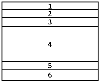
[0038] By selecting different materials and setting different film thickness parameters, the single crystal silicon heterojunction solar cell based on no gate lines and no doped contacts of the present invention can be flexibly designed, and can be prepared by using a variety of different film deposition methods Batteries, including but ...


PUM

PropertyMeasurementUnit
Thicknessaaaaaaaaaa
Widthaaaaaaaaaa
Thicknessaaaaaaaaaa

Abstract

The invention discloses a grid-line-free and undoped-contact based monocrystalline silicon heterojunction solar cell. The solar cell successively comprises an antireflection film, an ultrathin metal film, hole selective contact, monocrystalline silicon, electron selective contact and a back electrode from top to bottom. The ultrathin metal film is a continuous film, and a thickness is less than 10nm. The hole selective contact and the electron selective contact can be two layers or one layer respectively. In the invention, the ultrathin metal film is introduced so that a shielding effect of agrid line electrode in a traditional cell on sunlight is avoided, collection efficiency of a photon-generated carrier is improved, a limiting effect on long-waveband sunlight is enhanced, and a short-circuit current of the cell can be greatly improved; the metal film can also improve stability of the cell and increase flexibility of the cell; and the whole cell is simple in structure, flexible indesign, and simple in process, an extra doping process is not needed, an electrode pattern structure does not need to be defined, a process temperature can be controlled within 100 DEG C, and cost islow.

Description

technical field [0001] The invention relates to the field of solar photovoltaic technology, in particular to a single-crystal silicon heterojunction solar cell based on no grid lines and no doped contacts. Background technique [0002] Monocrystalline silicon solar cells occupy the most important photovoltaic market in the world and are an important photovoltaic technology solution. The traditional monocrystalline silicon photovoltaic technology is represented by two kinds of solar cells, homojunction and heterojunction. The former adopts p+ type hole selective contact and n+ type electron selective contact formed by diffusion doping; Crystalline silicon is used as a passivation layer, and p+ type and n+ type heavily doped amorphous silicon are used as hole and electron selective contacts. These doped contact technologies have many disadvantages: From a physical perspective, heavy doping will inevitably lead to unfavorable factors such as Auger recombination, narrowing of t...

Claims


Application Information

Patent Timeline
IPC IPC(8): H01L31/0224H01L31/0216H01L31/074
CPCH01L31/02167H01L31/02168H01L31/022425H01L31/022491H01L31/074Y02E10/50
Inventor 杨柳何赛灵
Owner ZHEJIANG UNIV
Why Eureka
Try Eureka