Full-oxide lead-free ferroelectric photovoltaic device with sandwich structure and preparation method thereof
A ferroelectric photovoltaic and oxide technology, which is applied in chemical instruments and methods, photovoltaic power generation, electrical components, etc., can solve the problems of reducing photovoltage and restrictions on the use of ferroelectric materials, so as to reduce recombination, improve photoelectric conversion performance, effect of promoting separation
- Summary
- Abstract
- Description
- Claims
- Application Information
AI Technical Summary
Problems solved by technology
Method used
Image
Examples
Embodiment 1
[0041] 1. Base cleaning
[0042] The Nb:STO substrate material was washed with a neutral detergent, then rinsed with deionized water, and then the substrate material was placed in acetone, absolute ethanol and deionized water for 15 minutes and then dried with high-purity nitrogen gas.
[0043] 2. Preparation of BFO layer
[0044] 1) Prepare precursor solution
[0045] Bi(NO 3 ) 3 ∙5H 2 O solid powder was added to glacial acetic acid (CH 3 COOH) (Bi: glacial acetic acid molar ratio is 1:8), continuously stirred on a magnetic stirrer for 8 h, and kept the temperature at 40-50 °C until the solution was a transparent solution, and the Bi(NO 3 ) 3 ∙5H 2 Fe(NO 3 ) 3 ∙9H 2 O was added to the above solution, and continuously stirred on a magnetic stirrer for 2h until the Fe(NO 3 ) 3 ∙9H 2 After O is completely dissolved. Then add polyethylene glycol 20000, polyethylene glycol 400 and citric acid according to the molar ratio of bismuth ferrite: polyethylene glycol 20000:...
Embodiment 2
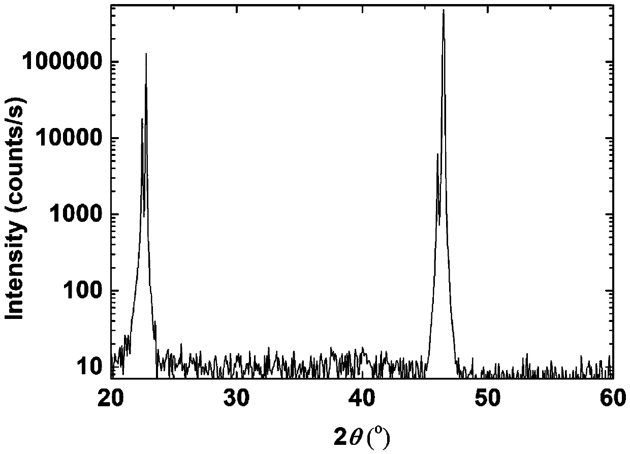
[0058] The device is prepared according to the method of Example 1, the difference is: when preparing the BFO layer, the temperature in the furnace during the heat treatment N 2 The flow rate is 0.1 L / min.
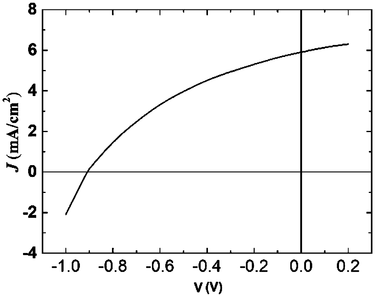
[0059] The BFO in the obtained device has good epitaxial growth, and the crystallinity of the BFO layer is good. Using the method of Example 1 to test the current and voltage performance of the device under light conditions, the open circuit voltage is 0.74 V, and the short circuit current is 5.2 mA / cm 2 , the photoelectric conversion efficiency reaches 1.4%.
Embodiment 3
[0061] Prepare the device according to the method of Example 1, the difference is: when preparing the BFO layer, the first layer of film is thrown off at a speed of 7000rpm, and the time is 2 minutes; the second to third layer of film is thrown off at a speed of 5000rpm, and the time is 1 Minutes, other layers of film are flung at a speed of 6000rpm, and the time is 1 minute.
[0062] The BFO in the obtained device has good epitaxial growth, and the crystallinity of the BFO layer is good. Adopt the method of embodiment 1 to test the current-voltage performance of device under light condition, its open circuit voltage is 0.85 V, and short circuit current is 5.6 mA / cm 2 , the photoelectric conversion efficiency reaches 1.8%.
PUM
| Property | Measurement | Unit |
|---|---|---|
| thickness | aaaaa | aaaaa |
| thickness | aaaaa | aaaaa |
| thickness | aaaaa | aaaaa |
Abstract
Description
Claims
Application Information
 - R&D
- Intellectual Property
- Life Sciences
- Materials
- Tech Scout
- Unparalleled Data Quality
- Higher Quality Content
- 60% Fewer Hallucinations
Browse by: Latest US Patents, China's latest patents, Technical Efficacy Thesaurus, Application Domain, Technology Topic, Popular Technical Reports.
© 2025 PatSnap. All rights reserved.Legal|Privacy policy|Modern Slavery Act Transparency Statement|Sitemap|About US| Contact US: help@patsnap.com


