Broad-spectrum photoelectric detector based on perovskite-carbon nanotube bulk heterojunction

A photodetector and carbon nanotube technology, applied in the field of wide-spectrum photodetectors, can solve the problems of wide-spectrum response exploration, photo-generated carrier recombination cannot be effectively avoided, etc., achieve high-response wide-spectrum light detection, help For efficient separation and overcoming the effect of low absorption

Inactive Publication Date: 2020-01-21
SUZHOU UNIV
View PDF10 Cites 3 Cited by
  • Summary
  • Abstract
  • Description
  • Claims
  • Application Information

AI Technical Summary

Problems solved by technology

However, its broad spectral response has not been explored, and the device structure is also based on a double-layer heterojunction structure. The recombination of photogenerated carriers in the perovskite body cannot be effectively avoided, and no interface modification layer is introduced to regulate the energy level arrangement. To improve the carrier separation efficiency

Method used


Image

  • Broad-spectrum photoelectric detector based on perovskite-carbon nanotube bulk heterojunction
  • Broad-spectrum photoelectric detector based on perovskite-carbon nanotube bulk heterojunction
  • Broad-spectrum photoelectric detector based on perovskite-carbon nanotube bulk heterojunction

Examples


Embodiment 1

[0035] Example 1: Preparation of perovskite-carbon nanotube bulk heterojunction broad-spectrum photodetector

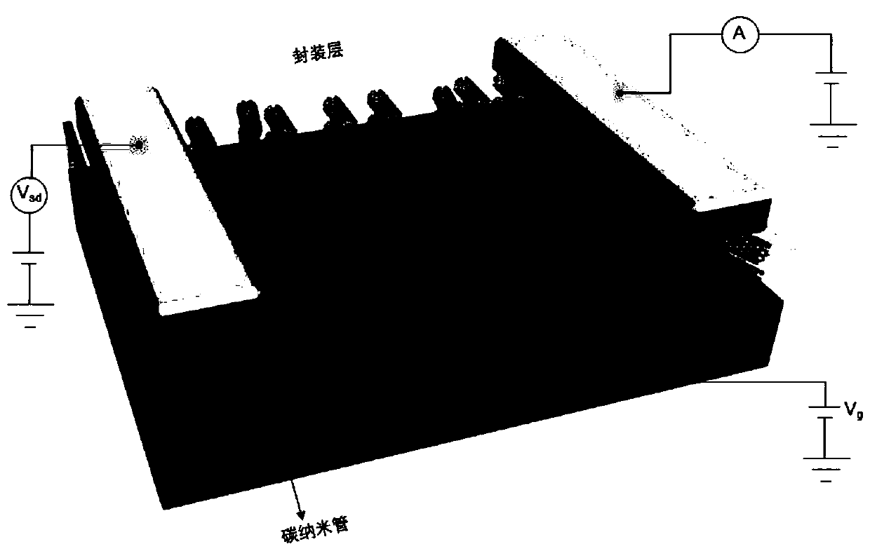
[0036] See image 3 In this embodiment, a perovskite-carbon nanotube bulk heterojunction wide-spectrum photodetector is provided, and the main preparation steps include:

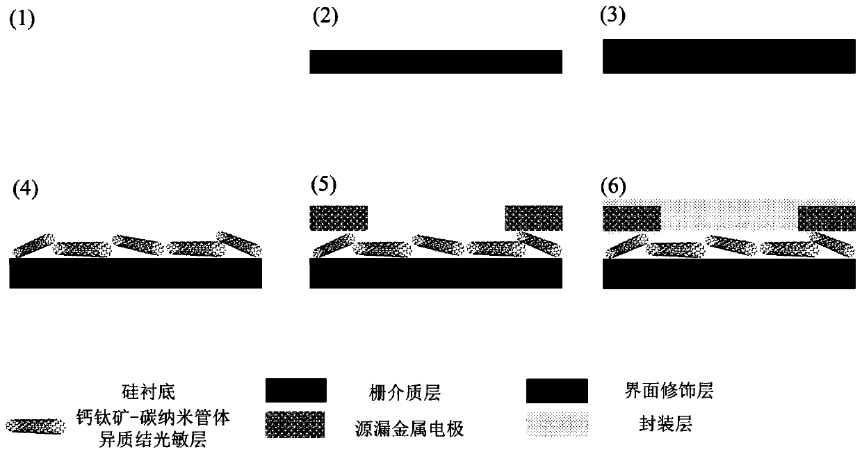
[0037] (1) Prepare N-type highly doped monocrystalline silicon wafers, clean them with standard RCA process, and dry them for later use;

[0038] (2) Transfer the cleaned monocrystalline silicon wafer to the growth equipment, and use thermal oxidation to grow a 300nm silicon dioxide gate dielectric layer;

[0039] (3) A 10nm titanium oxide interface modification layer is grown by atomic layer deposition;

[0040] (4) Weigh a certain amount of semiconducting carbon nanotube powder, purify it, and then modify the surface of the treated carbon nanotubes: weigh 100mg of the carbon nanotubes prepared and place them in a three-necked bottle And add 2.6g of 1,6-ethylenediamine in a three-necked flask, place it in a...

Embodiment 2

[0045] Example 2: Preparation of patterned perovskite-carbon nanotube bulk heterojunction broad-spectrum photodetector

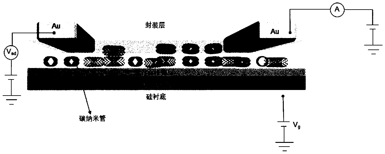
[0046] See Figure 4 In this embodiment, a patterned perovskite-carbon nanotube bulk heterojunction broad-spectrum photodetector is provided, and the main preparation steps include:

[0047] (1) Prepare N-type highly doped monocrystalline silicon wafers, clean them with standard RCA process, and dry them for later use;

[0048] (2) Transfer the cleaned monocrystalline silicon wafer to a growth device, and grow a 300nm silicon dioxide gate dielectric layer by thermal oxidation;

[0049] (3) A 10nm titanium oxide interface modification layer is grown by atomic layer deposition;

[0050] (4) Configure Poly-TPD chlorobenzene precursor, with a concentration of 20mg / mL, spin-coated on the substrate at 4000 rpm, spin-coating time is 40s, and place it on a hot plate at 100°C for 10 minutes to anneal and crystallize;

[0051] (5) Define the pattern of the perovskite photosensi...


PUM

PropertyMeasurementUnit
thicknessaaaaaaaaaa
thicknessaaaaaaaaaa
thicknessaaaaaaaaaa

Abstract

The invention discloses a broad-spectrum photoelectric detector based on a perovskite-carbon nanotube bulk heterojunction. The photoelectric detector comprises a substrate, a gate dielectric layer, aninterface modification layer, a perovskite-carbon nanotube bulk heterojunction film, an electrode layer and a packaging layer which are stacked in sequence, wherein a carbon nano tube in the perovskite-carbon nano tube bulk heterojunction thin film is a semiconductor carbon nano tube. According to the invention, the characteristics of high carrier mobility and wide-spectrum absorption of the carbon nano tube are utilized, so the absorption spectrum of perovskite is broadened to a near-infrared range, the crystallization quality and carrier mobility of the perovskite thin film are improved, and the key application bottleneck that the polycrystalline perovskite thin film prepared by a solution method is low in absorption and carrier mobility in the near-infrared range is overcome. The perovskite-carbon nanotube bulk heterojunction structure disclosed by the invention can remarkably increase the interface area for charge separation, so the photoresponsivity is greatly improved.

Description

Technical field [0001] The invention relates to the technical field of optoelectronic devices, in particular to a wide-spectrum photodetector based on a perovskite-carbon nanotube bulk heterojunction. Background technique [0002] A single photodetector can realize high-performance optical detection in a wide spectral range, and has broad application prospects in the fields of optical communication, clock monitoring, and spectral analysis. In the traditional sense, photodetectors that detect optical signals in different bands can only be based on a single semiconductor material with different band gaps, that is, a single material corresponds to a single detection band. In order to achieve wide-spectrum detection, it is necessary to integrate multiple photodetectors suitable for detecting different wavebands, and to ensure that these detectors work synchronously through the back-end system design, which leads to the complexity of the device structure, back-end processing circuit a...

Claims


Application Information

Patent Timeline
Patent Type & Authority Applications(China)
IPC IPC(8): H01L51/42H01L51/46
CPCH10K85/221H10K30/30H10K30/65H10K30/354Y02E10/549
Inventor 徐建龙张景越陈彤王穗东高旭
Owner SUZHOU UNIV
Why Eureka
Try Eureka