

LIGBT with carrier storage region
A technology of carrier storage and drift region, applied in LIGBT. It can solve the problem of long turn-off time of LIGBT, and achieve the effect of shortening the turn-off time and life.
- Summary
- Abstract
- Description
- Claims
- Application Information
AI Technical Summary
Problems solved by technology
Method used
Image

Examples
Embodiment 1
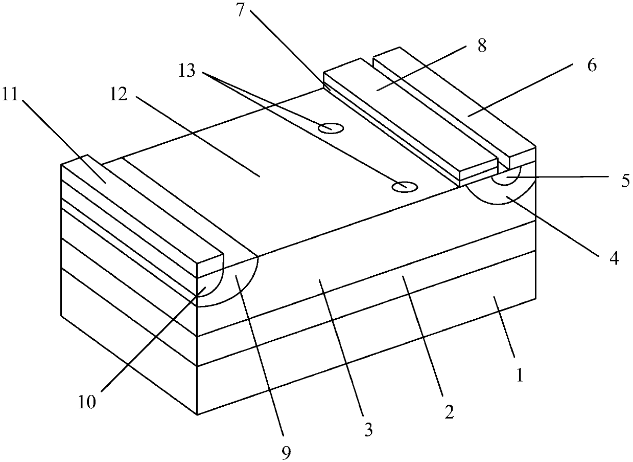
[0025] This embodiment provides a LIGBT with a carrier storage area, figure 1 A schematic structural diagram of this embodiment is shown. see figure 1 , the LIGBT of this embodiment includes a substrate 1, a buried oxide layer 2, an N-type drift region 3, a P well 4 located at one end of the N-type drift region 3, and an N-type heavily doped layer above the P well 4 from bottom to top. Region 5, the emitter 6 located above the P well 4 and the N-type heavily doped region 5, the gate dielectric layer 7 located above the P well 4, the gate 8 located above the gate dielectric layer 7, and the N-type drift region 3 An N-type buffer zone 9 at one end, a P-type heavily doped region 10 above the N-type buffer region 9 , and a collector 11 above the P-type heavily doped region 10 .
[0026] Wherein, the N-type drift region 3 includes an N-type silicon strip 12 parallel to the channel length direction of the LIGBT, and the N-type silicon strip 12 includes a carrier storage region 13,...
Embodiment 2
[0033] The LIGBT with the carrier storage region provided in this embodiment is a further improvement on Embodiment 1. In this embodiment, the P well 4 of the LIGBT can be formed by, but not limited to, ion implantation, diffusion, evaporation, and sputtering. And it is doped with aluminum ions and / or gallium ions, wherein the concentration and depth of doping of aluminum ions and / or gallium ions can be customized according to actual applications.
[0034] In this embodiment, the P-well 4 can also be doped with boron ions through, but not limited to, ion implantation, diffusion, evaporation, and sputtering.
[0035] In this embodiment, due to the large diffusion coefficient of aluminum and gallium, low diffusion temperature, and fast diffusion speed, the formed PN junction is a graded junction rather than an abrupt junction, so the breakdown voltage is relatively high. The LIGBT of this embodiment Higher reliability.
Embodiment 3
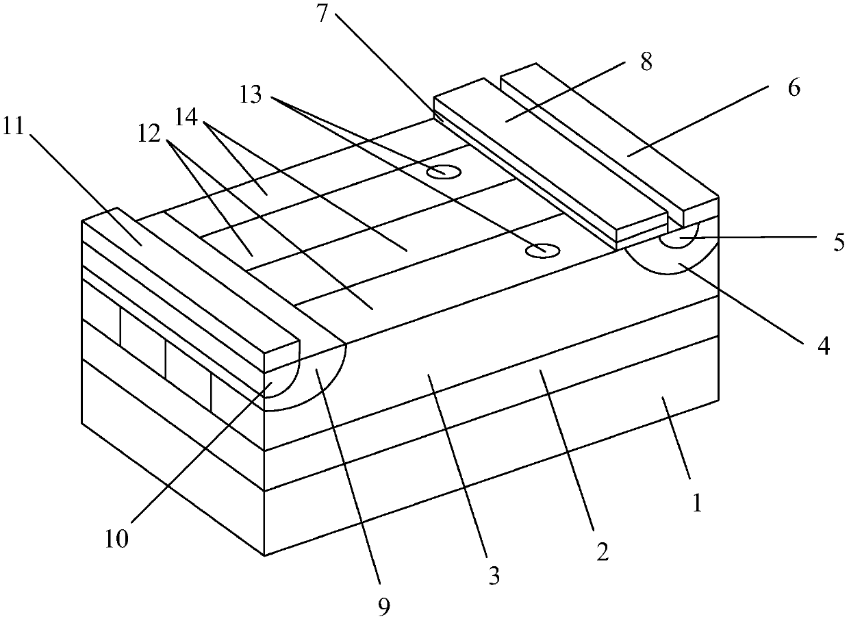
[0037] The LIGBT with carrier storage region provided in this embodiment is a further improvement on Embodiment 1, figure 2 A schematic structural diagram of this embodiment is shown. see figure 2 The improvement of this embodiment compared with Embodiment 1 is that the N-type drift region 3 of the LIGBT in this embodiment also includes a P-type silicon strip 14 parallel to the channel length direction of the LIGBT and spaced from the N-type silicon strip 12, forming A superjunction LIGBT. Wherein, the number of P-type silicon strips 14 can be customized according to actual applications.
[0038] The N-type drift region of the superjunction LIGBT of this embodiment includes N-type silicon strips, and the N-type silicon strips include a carrier storage region doped with hydrogen ions, so that the carrier storage region can be expressed as holes The barrier layer can reduce the saturation voltage drop Vcesat when the super-junction LIGBT is conducting forward, and can also ...
PUM
 Abstract
Description
Claims
Application Information