Single crystal thin film composite substrate and manufacturing method thereof

A single crystal thin film, composite substrate technology, applied in semiconductor/solid-state device manufacturing, electrical components, circuits, etc., can solve problems such as warping, affecting the efficiency of lithography process, electrodes, semiconductor performance, etc. Effect

Pending Publication Date: 2020-02-21
JINAN JINGZHENG ELECTRONICS
View PDF6 Cites 12 Cited by
  • Summary
  • Abstract
  • Description
  • Claims
  • Application Information

AI Technical Summary

Problems solved by technology

In the lithium niobate thin film composite substrate, there will be some warpage due to heterogeneous bonding (two films of different materials are combined together, due to the difference in thermal expansion coefficient, the degree of shrinkage after heating is different), which will affect the subsequent device processing craft
For example, the subsequent process is photolithography. If the substrate warpage is too large, the photolithography machine needs to be refocused every time it is stepped, which seriously affects the efficiency of the photolithography process.
[0004] In the prior art, a silicide layer is usually deposited on the back of the finished wafer or the substrate to improve the warped film, but if the warping of the film has reached a certain level, it is easy to deposit silicide on the back of the substrate. lead to more warping
In addition, in the prior art, plasma chemical vapor deposition is usually used to deposit silicide, but the temperature of plasma chemical vapor deposition is relatively high. If plasma chemical vapor deposition is used to deposit silicide on the back of the substrate, it is easy to damage the wafer. The film on the surface, and the performance of the electrodes, semiconductors and other devices on the wafer surface will also be affected
In addition, due to the piezoelectricity of the lithium niobate film, if silicide is deposited on the back of the finished lithium niobate film, the silicide will exert stress (pressure or tension) on the lithium niobate film, so that the refractive index of the lithium niobate film changes, which in turn affects the performance of lithium niobate thin films

Method used


Image

  • Single crystal thin film composite substrate and manufacturing method thereof
  • Single crystal thin film composite substrate and manufacturing method thereof
  • Single crystal thin film composite substrate and manufacturing method thereof

Examples


Embodiment 1

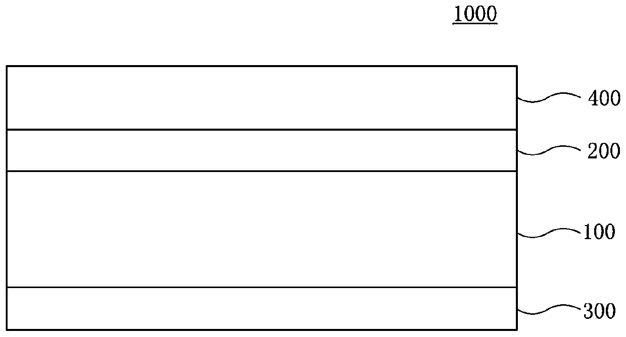
[0062] The base substrate is a single crystal lithium niobate wafer with a size of 3 inches and a thickness of 0.4 mm, and the lithium niobate wafer has a smooth surface. After the lithium niobate wafer is thoroughly cleaned, a silicon dioxide layer with a thickness of 2.7 μm is prepared on the upper and lower sides of the lithium niobate wafer by PECVD, and the silicon dioxide layer is chemically and mechanically polished to 2 μm and the surface roughness is less than 0.5nm.

[0063] The original substrate was a 3-inch lithium niobate wafer. Using ion implantation method, the implant dose of lithium niobate wafer is 4×10 16 ions / cm 2 the helium ion (He 1+), the energy of the helium ion is 200keV. After the ions are implanted into the lithium niobate wafer, a thin film layer, a separation layer and a residue layer are formed. At room temperature, the silicon dioxide layer on one surface of the single crystal lithium niobate wafer is bonded to the thin film layer of the li...

Embodiment 2

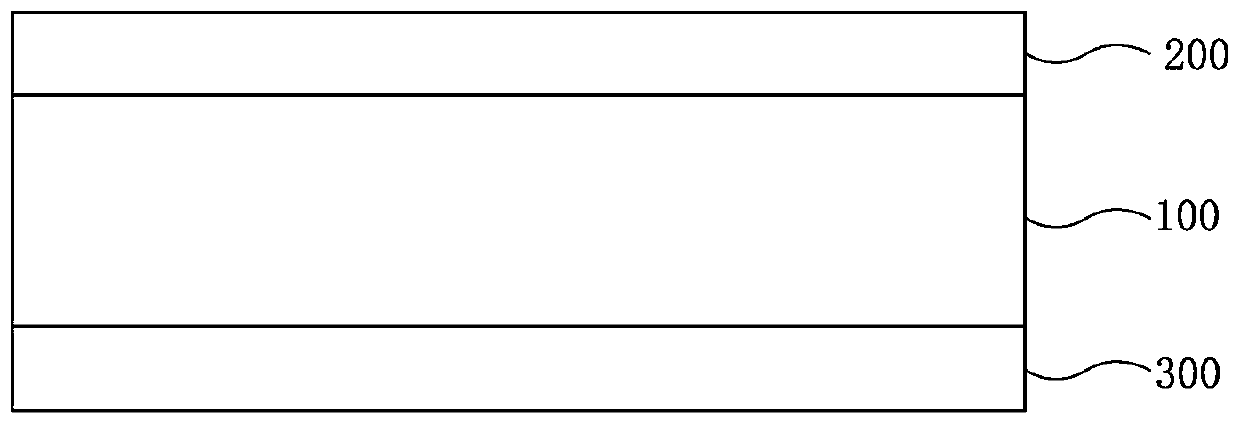
[0065] Substrate The substrate is a single crystal silicon wafer with a size of 3 inches and a thickness of 0.4 mm, and the single crystal silicon wafer has a smooth surface. After the single crystal silicon wafer is thoroughly cleaned, a silicon dioxide layer with a thickness of 2 μm and a surface roughness of less than 0.5 nm is prepared on the upper and lower sides of the single crystal silicon wafer by a thermal oxidation process.

[0066] The original substrate was a lithium niobate wafer measuring 3 inches. Using the ion implantation method, the implantation dose to the lithium niobate wafer is 4×10 16 ions / cm 2 Helium ions (He 1+ ), the energy of the helium ion is 200keV. After the ions are implanted into the lithium niobate wafer, a thin film layer, a separation layer and a residue layer are formed. At room temperature, the silicon dioxide layer on one surface of the single crystal silicon wafer is bonded to the thin film layer of the lithium niobate wafer to form ...

Embodiment 3

[0068] The substrate is a single crystal lithium niobate wafer with a size of 3 inches and a thickness of 0.4 mm, and the lithium niobate wafer has a smooth surface. After the lithium niobate wafer was thoroughly cleaned, a silicon nitride layer with a thickness of 2.7 μm was prepared on the upper and lower sides of the lithium niobate wafer by PECVD, and the silicon nitride layer was chemically and mechanically polished to 2 μm and the surface roughness was less than 0.5nm.

[0069] The original substrate was a lithium niobate wafer measuring 3 inches. Using the ion implantation method, the implantation dose to the lithium niobate wafer is 4×10 16 ions / cm 2 Helium ions (He 1+ ), the energy of the helium ion is 200keV. After the ions are implanted into the lithium niobate wafer, a thin film layer, a separation layer and a residue layer are formed. At room temperature, the silicon nitride layer on one surface of the single crystal lithium niobate wafer is bonded to the thi...


PUM

PropertyMeasurementUnit
thicknessaaaaaaaaaa
thicknessaaaaaaaaaa
thicknessaaaaaaaaaa

Abstract

The invention discloses a single crystal thin film composite substrate and a manufacturing method thereof. The single crystal thin film composite substrate comprises an underlayer substrate, an isolation layer, a compensation layer and a single crystal thin film functional layer, wherein the isolation layer is located on the underlayer substrate; the compensation layer is located below the underlayer substrate; and the single crystal thin film functional layer is located on the isolation layer, and the isolation layer and the compensation layer are made of the same material. According to the invention, the defect of obvious warpage of the underlayer substrate in the single crystal thin film composite substrate is solved. Meanwhile, the tedious preparation process is avoided, and the process cost is reduced.

Description

technical field [0001] The invention relates to a single crystal thin film composite substrate with improved warpage and a method for manufacturing the single crystal thin film composite substrate, in particular, to a single crystal thin film composite substrate with improved wafer warpage and a method for manufacturing the same A method for a single crystal thin film composite substrate. Background technique [0002] Piezoelectric thin film materials such as lithium niobate film and lithium tantalate film have excellent nonlinear optical properties, electro-optic properties, and acousto-optic properties, and are widely used in the fields of optical signal processing, information storage and other electronic devices. Lithium niobate films and lithium tantalate films have strongly guided high refractive index contrast structures, so they can be used as substrates to provide material support for optoelectronic structures realized in a small volume range. [0003] Lithium niob...

Claims


Application Information

Patent Timeline
Patent Type & Authority Applications(China)
IPC IPC(8): H01L21/02H01L21/18
CPCH01L21/0201H01L21/02104H01L21/185
Inventor 张秀全朱厚彬罗具廷李真宇
Owner JINAN JINGZHENG ELECTRONICS
Why Eureka
Try Eureka