
A crystal growth method based on vgf method for vapor phase doping

A technology of crystal growth and gas phase doping, applied in the direction of crystal growth, single crystal growth, single crystal growth, etc., can solve the problems of destroying crystal uniformity and integrity, uneven distribution of Fe, reducing device performance, etc., to improve uniformity performance and crystallization rate, cost saving, and the effect of reducing the amount of doping

Active Publication Date: 2021-10-12
珠海鼎泰芯源晶体有限公司
View PDF3 Cites 0 Cited by
  • Summary
  • Abstract
  • Description
  • Claims
  • Application Information

AI Technical Summary

Problems solved by technology

[0005] In addition, the existing technology is to directly mix the dopant Fe with the indium phosphide polycrystalline material and simultaneously heat up, and the dopant Fe and the indium phosphide polycrystalline material are mixed in a molten state; during the heating stage of crystal growth, the temperature is raised If the rate is too fast, the mixing of Fe element and indium phosphide polycrystal in the form of molten state will make the distribution of Fe in the indium phosphide melt uneven, thus destroying the uniformity and integrity of the crystal
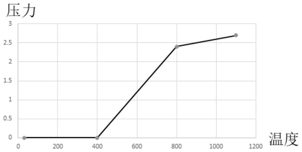
[0006] Furthermore, the crystal growth process is generally divided into a heating stage (heating to the melting point of indium phosphide polycrystalline), a constant temperature stage (indium phosphide polycrystalline is gradually converted into a melt, and Fe diffuses into the indium phosphide melt at the same time) and a cooling stage (crystallization stage); in the prior art, the heating rate of the heating stage is faster, so more iron will be precipitated, causing Fe in the semi-insulating InP substrate to diffuse to the epitaxial layer during the epitaxial growth process, thereby reducing the use of InP single The performance of crystal-fabricated devices

Method used


Image

  • A crystal growth method based on vgf method for vapor phase doping
  • A crystal growth method based on vgf method for vapor phase doping
  • A crystal growth method based on vgf method for vapor phase doping

Examples


Embodiment Construction

[0051] The present invention will be further described in detail below in conjunction with the accompanying drawings and specific embodiments.

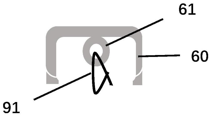
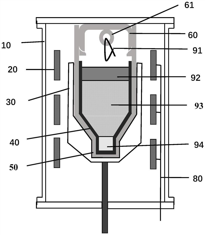
[0052] In combination with 1 and 2, this embodiment provides a crystal growth device and a crystal growth method for growing an indium phosphide single crystal by vapor phase doping of iron element based on the VGF method.

[0053] Among them, such as figure 2 , the crystal growth device comprises a growth furnace 10, a graphite crucible holder 20, a boron nitride crucible 40, a quartz tube 50, and a quartz cap 60; several heating devices 30 are sequentially arranged in the growth furnace 10 from bottom to top; each heating device passes The galvanic couple 80 is connected to the control system; the graphite crucible holder 20 is located in the growth furnace 10 . Wherein the bottom of the boron nitride crucible 40 has a seed crystal plug for carrying the seed crystal.

[0054] During crystal growth, various raw materials are place...


PUM


Abstract

The invention discloses a crystal growth method based on a VFG method for gas phase doping, and relates to the technical field of crystal preparation. The method includes the following steps: S1, putting polycrystals, seed crystals, and red phosphorus into the crucible for crystal growth; S2, placing the crucible in a quartz tube; it is characterized in that, after step S2, it also includes, S3, connecting the doped A quartz sealing cap of the dopant is covered on the quartz tube, and the dopant is located in the quartz tube, and the dopant is not in contact with the polycrystal, the seed crystal and the red phosphorus; The quartz tube is sealed. Through the improvement of the quartz capping and heating process used for VGF crystal growth, the dopant is separated from other raw materials for crystal growth, and the dopant Fe element enters the melt through gas phase diffusion to achieve uniform doping concentration. The uniformity of the crystal resistivity and the crystal formation rate are improved; meanwhile, the doping amount of the dopant Fe can be reduced, and the cost is saved.

Description

technical field [0001] The invention relates to the technical field of crystal preparation, in particular to a crystal growth method based on gas phase doping by a VGF method. Background technique [0002] The compound semiconductor InP material has high electron mobility and a large band gap. As a new electronic functional material, it can be widely used in long-wave optical fiber communication technology, microwave, millimeter-wave devices, and space radiation-resistant solar cells. With the increasing maturity of InP-based microelectronics manufacturing technology, more attention has been paid to the application of semi-insulating SI-InP in high-frequency components and optoelectronic integrated circuits. Therefore, obtaining InP-based semiconductor substrate materials with excellent properties has a great impact on the quality of devices. crucial role. [0003] At present, indium phosphide (InP) single crystals with high quality and low defect density are mainly prepare...

Claims


Application Information

Patent Timeline
Patent Type & Authority Patents(China)
IPC IPC(8): C30B11/06C30B29/40C30B11/00
CPCC30B11/003C30B11/006C30B11/06C30B29/40
Inventor 赵有文段满龙刘鹏卢伟杨俊刘京明谢辉
Owner 珠海鼎泰芯源晶体有限公司
Learn More