Transparent thin film transistor device based on zirconium oxide and lanthanum oxide and preparation method thereof

A transparent film and lanthanum oxide technology, which is applied in semiconductor/solid-state device manufacturing, transistors, semiconductor devices, etc., can solve problems such as inability to mass-produce, high manufacturing cost, and unguaranteed performance of TFT devices, and achieve large-scale industrial Application, process compatibility, effect of reducing absorption

Pending Publication Date: 2020-05-08
XIAN JIAOTONG LIVERPOOL UNIV
View PDF4 Cites 3 Cited by
  • Summary
  • Abstract
  • Description
  • Claims
  • Application Information

AI Technical Summary

Problems solved by technology

However, most of the existing preparation methods are expensive and cannot be mass-produced, or the performance of TFT devices cannot be guaranteed

Method used


Image

  • Transparent thin film transistor device based on zirconium oxide and lanthanum oxide and preparation method thereof
  • Transparent thin film transistor device based on zirconium oxide and lanthanum oxide and preparation method thereof
  • Transparent thin film transistor device based on zirconium oxide and lanthanum oxide and preparation method thereof

Examples


preparation example Construction

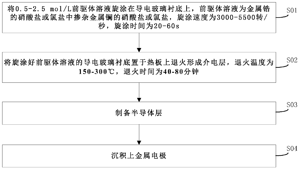
[0034] Such as figure 1 As shown, the present invention discloses a method for preparing a transparent thin film transistor device based on zirconia and lanthanum oxide, comprising the following steps:

[0035] S01: Spin-coat a 0.5-2.5 mol / L precursor solution on a conductive glass substrate. The precursor solution is the nitrate or chloride salt doped with metal lanthanum in the nitrate or chloride salt of metal zirconium, and the nitrate or chloride salt doped with metal lanthanum. The concentration of nitrate or chloride salt accounts for 0-50% of the total concentration, the spin-coating speed is 3000-5500 rpm, and the spin-coating time is 20-60s;

[0036] S02: Place the conductive glass substrate spin-coated with the precursor solution on a hot plate to anneal to form a dielectric layer, the annealing temperature is 150-300°C, and the annealing time is 40-80 minutes;

[0037] S03: Prepare a semiconductor layer; including:

[0038] The semiconductor precursor drug is dis...

Embodiment 1

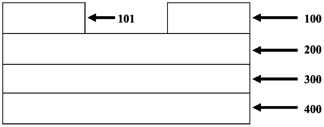
[0048] Such as figure 2 As shown, a transparent TFT device based on zirconia and lanthanum oxide includes a conductive glass substrate 400, a dielectric layer 300, a semiconductor layer 200, an upper metal electrode (100, 101), and an upper metal electrode (100, 101); The electrodes include a source electrode 100 and a drain electrode 101, the conductive material of the conductive glass substrate is indium tin oxide, the material of the semiconductor layer is selected from indium oxide, and the upper metal electrode is indium tin oxide.

[0049] Its preparation method, concrete steps comprise:

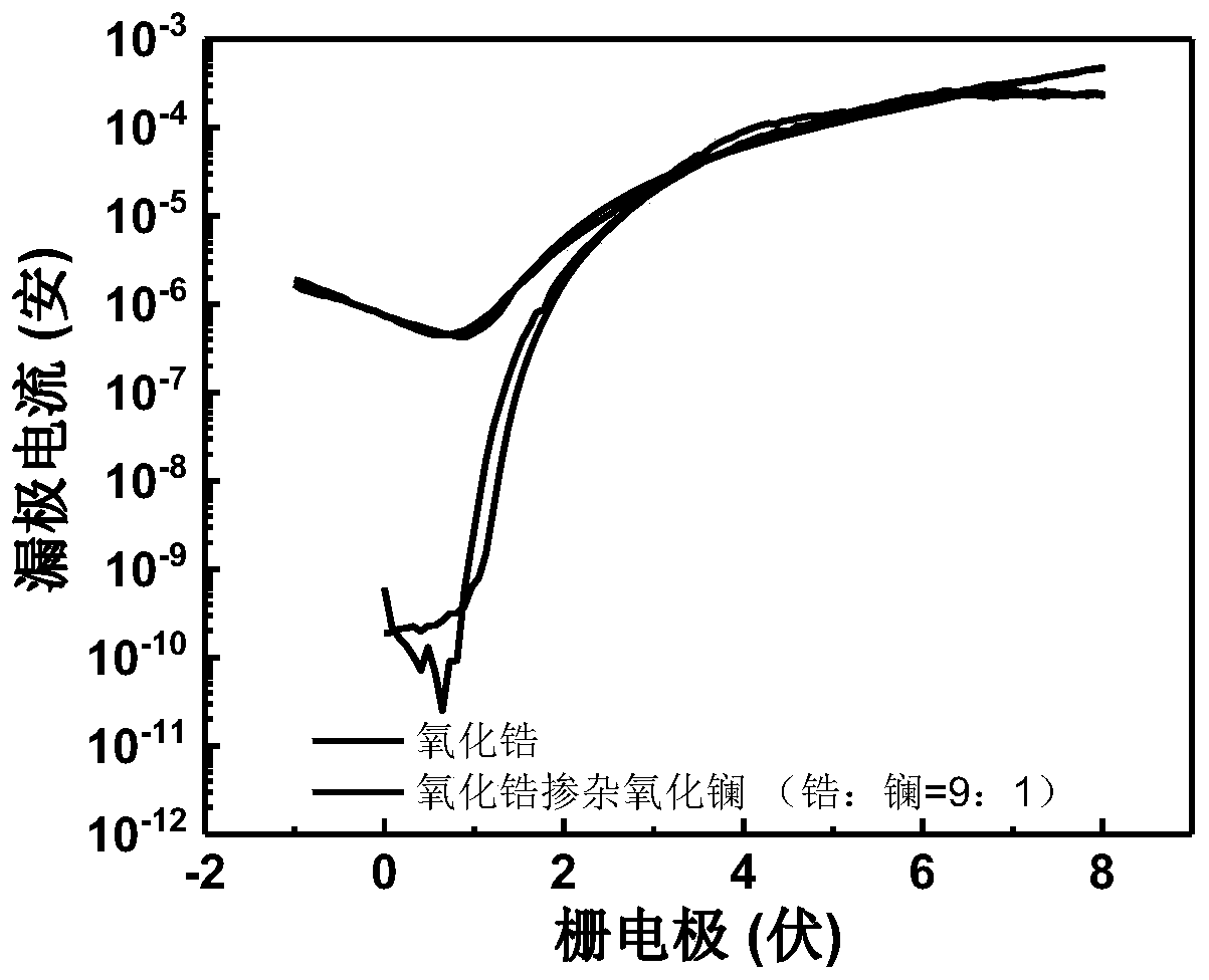
[0050] a) Dissolve the precursor drug in the aqueous solution to obtain a precursor solution with a concentration of 2.5mol / L. The precursor drug is doped with zirconium nitrate and lanthanum nitrate, and the ratio of the two is 9:1;

[0051] b) Sonicate the precursor solution for 15 minutes;

[0052]c) Clean the conductive glass substrate. The conductive material of the conductive ...

Embodiment 2

[0060] Such as Figure 4 As shown, a transparent TFT device based on zirconia and lanthanum oxide includes a conductive glass substrate 800, a dielectric layer 700, a semiconductor layer 600, and an upper metal electrode arranged sequentially from bottom to top; the upper metal electrode includes a source electrode 500 and the drain electrode 501; the conductive material of the conductive glass substrate is indium tin oxide; the material of the semiconductor layer is selected from zinc oxide, and the upper metal electrode is indium tin oxide.

[0061] Its preparation method, concrete steps comprise:

[0062] a) Dissolve the precursor drug in the aqueous solution to obtain a precursor solution with a concentration of 2.5mol / L. The precursor drug is doped with zirconium chloride and lanthanum chloride, and the ratio of the two is 9:1;

[0063] b) Sonicate the precursor solution for 15 minutes;

[0064] c) To clean the conductive glass substrate, immerse the conductive glass su...


PUM


Abstract

The invention discloses a transparent thin film transistor device based on zirconium oxide and lanthanum oxide, which comprises a conductive glass substrate, a dielectric layer, a semiconductor layerand an upper metal electrode which are sequentially arranged from bottom to top, the upper metal electrode comprises a source electrode and a drain electrode, and the dielectric layer is made of a mixed oxide of zirconium oxide and lanthanum oxide. The insulating layer and the semiconductor layer of the TFT are prepared by adopting a solution method, so that low-cost and large-area TFT preparationis realized, and equipment and raw material investment is relatively low; and the method is compatible with a traditional process in process, and the preparation cost can be effectively controlled.

Description

technical field [0001] The invention relates to the technical field of thin film transistors, in particular to a transparent thin film transistor device based on zirconia and lanthanum oxide and a preparation method thereof. Background technique [0002] Thin-film transistors (TFT) have broad prospects in the display field. Thin-film transistor technology has developed from the original a-Si (amorphous silicon) thin-film transistors to the current LTPS (polysilicon) thin-film transistors, MILC thin-film transistors, and oxide thin-film transistors. The light-emitting technology has also developed from the original LCD and PDP to the current OLED (Organic Light-Emitting Display). [0003] There are many traditional methods for preparing thin film transistors, such as atomic layer deposition, magnetron sputtering, physical vapor deposition, chemical vapor deposition and so on. [0004] For example, Chinese patent document CN 105609564 A discloses a thin film transistor manufa...

Claims


Application Information

Patent Timeline
Patent Type & Authority Applications(China)
IPC IPC(8): H01L29/786H01L29/51H01L21/445H01L21/34
CPCH01L29/7869H01L29/517H01L29/66969H01L21/445
Inventor 方欲晓赵春赵策洲杨莉
Owner XIAN JIAOTONG LIVERPOOL UNIV
Why Eureka
Try Eureka