

Method for preparing organic solar cell with vertical phase gradient distribution photoactive layer by oscillation-assisted spin-coating process
A technology of solar cells and photoactive layers, applied in photovoltaic power generation, circuits, electrical components, etc., can solve the problems of low photogenerated carrier transport and interface transfer efficiency, poor phase separation in the photoactive layer, and high carrier recombination Probability and other issues, to achieve the effect of optimizing the phase separation of the donor/acceptor inside the photoactive layer, increasing the electron mobility, and improving the contact situation
- Summary
- Abstract
- Description
- Claims
- Application Information
AI Technical Summary
Problems solved by technology
Method used
Image


Examples
Embodiment 1
[0034] Embodiment 1 (control group):
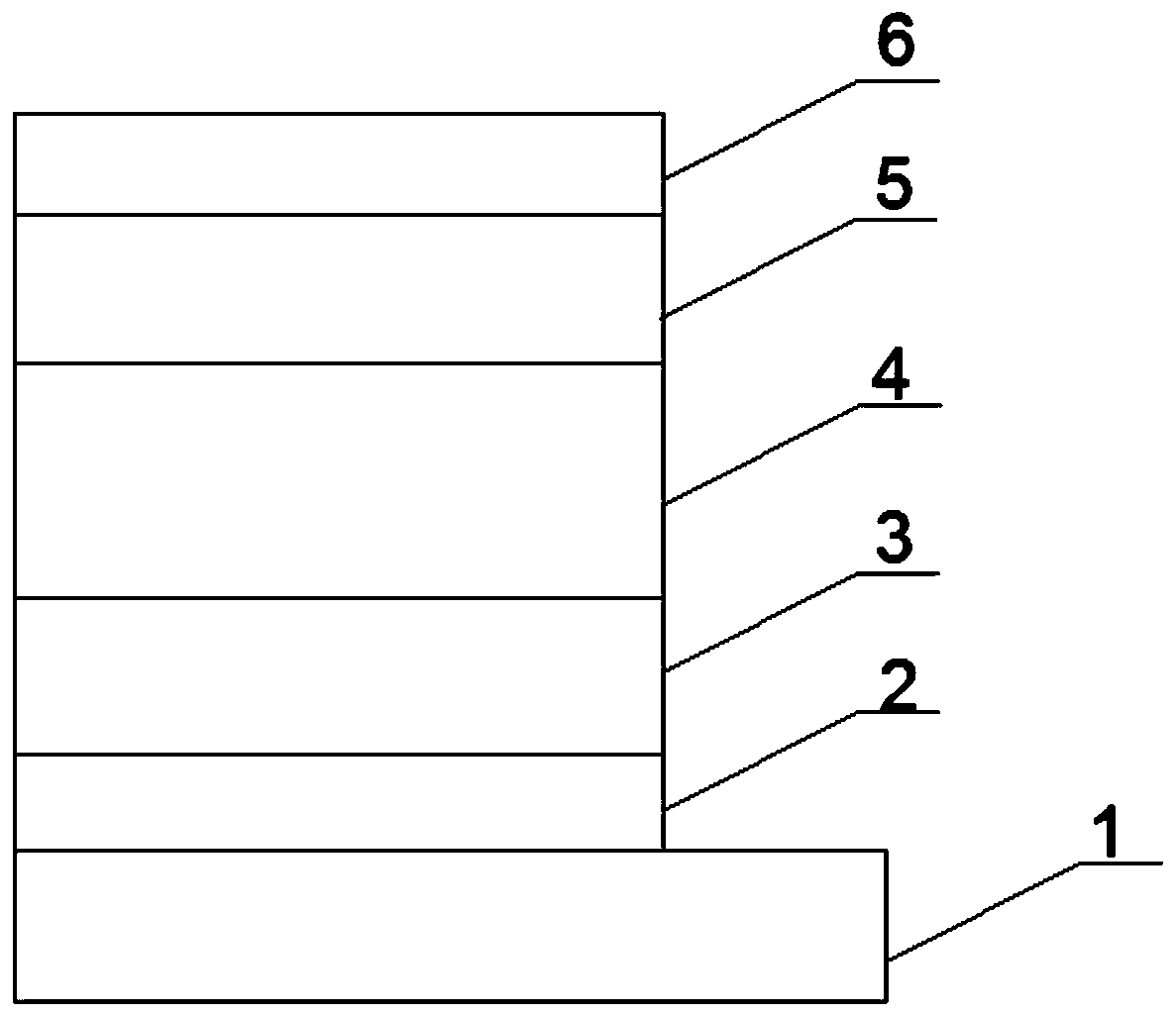
[0035] (1) Clean the substrate composed of the transparent substrate 1 and the transparent conductive cathode ITO 2 whose surface roughness is less than 1mm, and dry it with nitrogen after cleaning;
[0036] (2) Spin-coat ZnO (5000rpm, 50s, 40nm) on the surface of the transparent conductive cathode ITO 2 to prepare the cathode buffer layer 3, and perform thermal annealing on the formed film (200°C, 2h);
[0037] (3) PBDB-T:ITIC (1:1, 8mg / ml) solution was dripped on the cathode buffer layer 3, and the photoactive layer 4 was prepared by spin coating (2000rpm, 40s, 110nm);
[0038](4) PBDB-T at room temperature: ITIC photoactive layer 4 was placed in a glove box for 10 minutes;
[0039] (5) evaporate MoO on the photoactive layer 4 anode buffer layer 5 (15nm);
[0040] (6) Evaporate metal anode Ag (100nm) on the anode buffer layer;
[0041] (7) Under standard test conditions: AM 1.5, 100mW / cm 2 , the measured open circuit voltage (VOC) o...
Embodiment 2
[0043] (1) Clean the substrate composed of the transparent substrate 1 and the transparent conductive cathode ITO 2 with a surface roughness less than 1 nm, and dry it with nitrogen after cleaning;
[0044] (2) Spin-coat ZnO (5000rpm, 50s, 40nm) on the surface of the transparent conductive cathode ITO 2 to prepare the cathode buffer layer 3, and perform thermal annealing on the formed film (200°C, 2h);
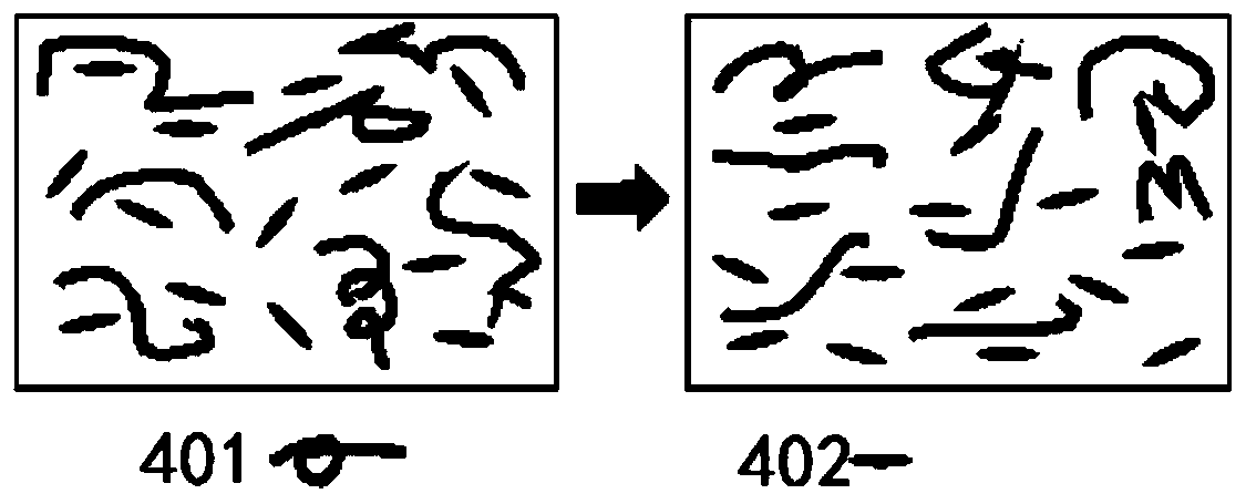
[0045] (3) PBDB-T:ITIC (1:1, 8mg / ml) solution was dripped on the cathode buffer layer 3, and the substrate was ultrasonically treated (1min, 20kHz);
[0046] (4) Prepare the photoactive layer 4 by spin coating process (2000rpm, 40s, 110nm);
[0047] (5) PBDB-T at room temperature: ITIC photoactive layer 4 was placed in a glove box for 10 minutes;
[0048] (6) evaporate MoO on the photoactive layer 4 anode buffer layer 5 (15nm);
[0049] (7) Evaporate metal anode Ag (100nm) on the anode buffer layer;
[0050] (8) Under standard test conditions: AM 1.5, 100mW / cm 2 , the meas...
Embodiment 3
[0052] (1) Clean the substrate composed of the transparent substrate 1 and the transparent conductive cathode ITO 2 with a surface roughness less than 1 nm, and dry it with nitrogen after cleaning;
[0053] (2) Spin-coat ZnO (5000rpm, 50s, 40nm) on the surface of the transparent conductive cathode ITO 2 to prepare the cathode buffer layer 3, and perform thermal annealing on the formed film (200°C, 2h);
[0054] (3) PBDB-T:ITIC (1:1, 8mg / ml) solution was dripped on the cathode buffer layer 3, and the substrate was ultrasonically treated (1min, 30kHz);
[0055] (4) Prepare the photoactive layer 4 by spin coating process (2000rpm, 40s, 110nm);
[0056] (5) PBDB-T at room temperature: ITIC photoactive layer 4 was placed in a glove box for 10 minutes;
[0057] (6) Evaporate MoO on the photoactive layer 4 3 Anode buffer layer 5 (15nm);
[0058] (7) Evaporate metal anode Ag (100nm) on the anode buffer layer;
[0059] (8) Under standard test conditions: AM 1.5, 100mW / cm 2 , the m...
PUM
| Property | Measurement | Unit |
|---|---|---|
| Thickness | aaaaa | aaaaa |
| Concentration | aaaaa | aaaaa |
| Thickness | aaaaa | aaaaa |
Abstract
Description
Claims
Application Information