GaN-based heterojunction integrated device structure and manufacturing method

A GaN-based, device structure technology, applied in semiconductor/solid-state device manufacturing, semiconductor devices, electrical components, etc., can solve problems such as low efficiency, small contact area between gate and AlGaN, device burnout failure, etc.

Active Publication Date: 2020-05-29
M MOS SEMICON HK
View PDF8 Cites 2 Cited by
  • Summary
  • Abstract
  • Description
  • Claims
  • Application Information

AI Technical Summary

Problems solved by technology

For devices with pGaN on the AlGaN surface, the pGaN gate can help to pick up the holes generated during breakdown, but the efficiency of this hole extraction is not high, because the gate pGaN is on the AlGaN, and the holes are on the AlGaN Between / GaN, pGaN and AlGAN are a heterojunction, the forbidden band of AlGaN is relatively wide, and the holes are relatively difficult to drift to pGaN to be drawn away, and the saturation speed of holes in AlGaN / GaN is relatively slow , it is not easy to drift from the breakdown point to the gate pGaN, and the contact area between the pGaN gate and AlGaN is not large, and the ability to receive holes is limited
If neither the gate nor the source can pick up the holes effectively and quickly, under high voltage reverse bias, these holes staying around the gate and source will cause the device to burn out and fail
At present, many gallium nitride devices avoid applications where breakdown occurs. They are mainly used for radio frequency power amplifiers or power factor correction (PFC) applications, but gallium nitride power devices will eventually overcome this problem. Otherwise, its application prospects will be greatly limited

Method used


Image

  • GaN-based heterojunction integrated device structure and manufacturing method
  • GaN-based heterojunction integrated device structure and manufacturing method
  • GaN-based heterojunction integrated device structure and manufacturing method

Examples


Embodiment 1

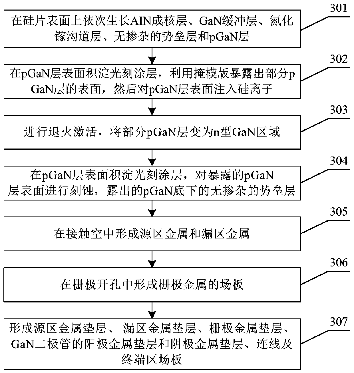
[0062] image 3 It is a flow chart of the manufacturing method of the gallium nitride-based heterojunction integrated device structure of the present invention, which will be referred to below image 3 , the method for manufacturing the GaN-based heterojunction integrated device structure of the present invention is described in detail.

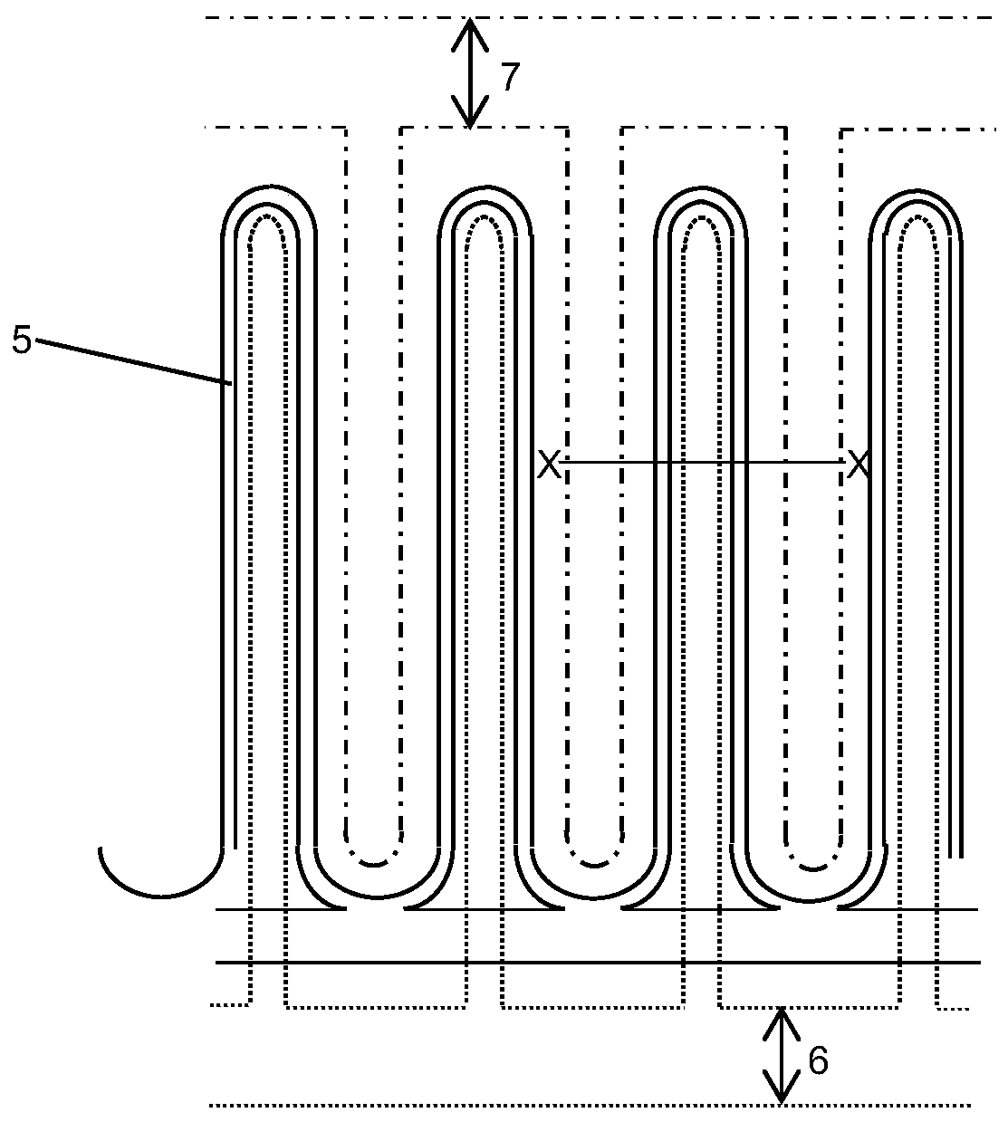
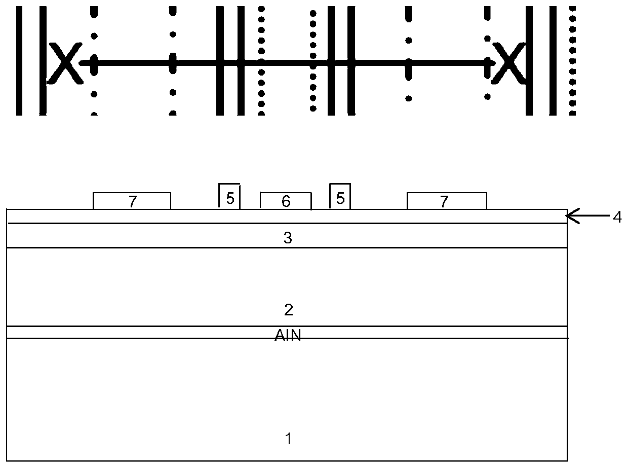
[0063] First, in step 301, an AlN nucleation layer, a GaN buffer layer 2, a gallium nitride channel layer (GaN Channel) 3, an undoped barrier layer 4 and a pGaN layer 5 are sequentially grown on the surface of the silicon wafer.

[0064] Figure 4 It is a schematic cross-sectional view of an embodiment of the present invention after all epitaxial layers are completed, such as Figure 4 As shown, in the embodiment of the present invention, a 200nm AlN nucleation layer, a 4um unintentionally doped GaN buffer layer 2, and a 300nm gallium nitride channel layer (GaNChannel) are sequentially grown on the surface of the silicon wafer 1 by the MOCV...

Embodiment 2

[0081] Figure 17 For the present invention connects the cross-section schematic diagram of each electrode in the integrated device structure with metal wire, as Figure 17 As shown, wherein, G is the gate of the transistor, S is the source of the transistor, D is the drain of the transistor, A is the anode of the gallium nitride-based pn junction diode, and C is the cathode of the gallium nitride-based pn junction diode.

[0082] The gallium nitride-based heterojunction field effect transistor structure of the present invention is to integrate a gallium nitride-based pn junction diode (GaN diode) on the original device, and the HEMT transistor in the integrated device can be integrated with the gallium nitride-based pn junction diode. The junction diodes are connected together with metal wires, for example, the drain D of the HEMT transistor is connected to the anode A of the GaN-based pn junction diode, and the source S of the HEMT transistor is connected to the cathode C of...


PUM

PropertyMeasurementUnit
thicknessaaaaaaaaaa
thicknessaaaaaaaaaa
thicknessaaaaaaaaaa

Abstract

The invention discloses a manufacturing method of a GaN-based heterojunction integrated device structure. The manufacturing method comprises the following steps of: sequentially growing an AIN nucleating layer, a GaN buffer layer, a GaN channel layer, an undoped barrier layer and a pGaN layer on the surface of a silicon wafer; depositing a photoetching coating on the surface of the pGaN layer, exposing a part of the surface of the pGaN layer by using a mask plate, and injecting silicon ions; annealing and activating the injected silicon ions, and changing the pGaN layer injected with the silicon ions into an n type GaN region; depositing a photoetching coating, etching the exposed pGaN layer by using a mask plate, exposing the undoped barrier layer, and forming a contact hole; forming an ohmic contact electrode in the contact hole; forming a gate opening, and forming a gate metal field plate in the gate opening; and forming a source region metal cushion layer, a drain region metal cushion layer, a grid electrode metal cushion layer, an anode metal cushion layer and cathode metal cushion layer of the GaN diode, a connecting wire and a terminal region field plate on the surface of the structure. The GaN-based heterojunction integrated device structure provided by the invention plays a role in protecting an original device.

Description

technical field [0001] The present invention relates to a GaN-based heterojunction field-effect transistor structure, more specifically to a GaN-based semiconductor integrated device integrated with GaN-based heterojunction transistors and GaN pn junction diodes structure and manufacturing method. Background technique [0002] The third generation of semiconductor materials, including CdS, ZnO, SiC, GaN, diamond, etc. The bandgap of these semiconductor materials is greater than 2.2eV. In terms of electronic devices, the research on SiC and GaN is relatively mature, and it is currently a hot spot in the field of semiconductor materials and device research in the world. [0003] Gallium nitride (GaN) has a bandgap width of 3.4eV, and silicon carbide (SiC) has a bandgap width of 3.3eV. Wide bandgap materials can withstand higher operating temperatures and greater breakdown electric fields than silicon semiconductor materials. A higher breakdown electric field means that the d...

Claims


Application Information

Patent Timeline
Patent Type & Authority Applications(China)
IPC IPC(8): H01L29/872H01L29/06H01L21/329
CPCH01L29/872H01L29/0684H01L29/66143H01L29/66075Y02P70/50
Inventor 欧阳伟伦梁安杰罗文健
Owner M MOS SEMICON HK
Why Eureka
Try Eureka