Diamond thin film of multi-level micro-nano structure and preparation method and application thereof
A technology of diamond film and nano-diamond, which is applied in metal material coating process, gaseous chemical plating, coating, etc., can solve the problems of time-consuming, complicated process, expensive RIE equipment, etc., and achieve long life, simple preparation process, good binding effect
- Summary
- Abstract
- Description
- Claims
- Application Information
AI Technical Summary
Problems solved by technology
Method used
Image

Examples
preparation example Construction
[0046] According to a second aspect of the present invention, a method for preparing a diamond film is provided, comprising the following steps:
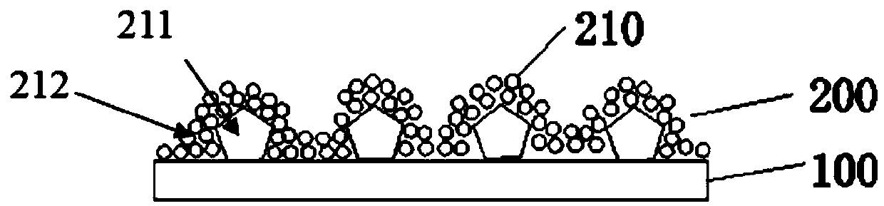
[0047] First, low-density crystal implantation is performed on the pretreated substrate, and diamond is grown once by chemical vapor deposition method; then high-density crystal implantation is performed on the primary diamond film growth, and diamond is grown secondary by chemical vapor deposition method, A diamond film is obtained.
[0048] Chemical vapor deposition methods include but are not limited to hot wire or microwave plasma enhanced chemical vapor deposition methods, preferably hot wire chemical vapor deposition methods.
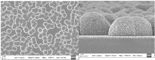
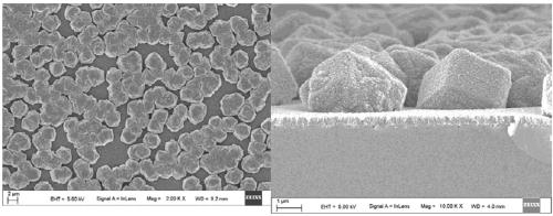
[0049] The chemical vapor deposition diamond growth needs to implant diamond seeds, and then carry out epitaxial growth at the implanted seed crystal point, and use the selective adsorption of diamond crystal seeds on the substrate to construct a super-hydrophobic micro-nano structure. The present inve...
Embodiment 1
[0087] Embodiment 1 matrix silicon
[0088] A method for preparing a diamond film, comprising the steps of:
[0089] (1) Clean the surface of the substrate silicon, first use deionized water to ultrasonically clean it twice, each time for 5 minutes, and finally use alcohol to ultrasonically clean it for 5 minutes, and dry it with nitrogen;
[0090] (2) Carry out etching treatment to the substrate silicon that cleans up, put the sample into 10ml 32%H 2 o 2 +10ml NH 3· h 2 O+50ml H 2 O solution, 80 degrees Celsius for 10 minutes;
[0091] (3) Carry out recleaning to matrix silicon, ultrasonic 3 times with deionized water, each time 5 minutes, dry with nitrogen at last;
[0092] (4) Carry out low-density crystal planting on the substrate silicon, put the substrate silicon into the low-density crystal-planting solution and ultrasonicate for 30 minutes, take it out, and dry it with nitrogen; the low-density crystal-planting solution is detonation nano-diamond suspension, and ...
Embodiment 2
[0097] Embodiment 2 copper alloy matrix
[0098] A method for preparing a diamond film, comprising the steps of:
[0099] (1) Clean the surface of the copper alloy substrate, first use deionized water to ultrasonically clean for 2 times, each time for 5 minutes, finally use alcohol to ultrasonically clean for 5 minutes, and dry with nitrogen;
[0100] (2) Carry out corrosion treatment to the cleaned copper alloy substrate, first ultrasonic cleaning in alkaline solution for 5 minutes, then cleaning in acid solution for 30 seconds, wherein the alkaline solution is 1M NaOH, and the acid solution is 4M HCl;
[0101] (3) Clean the copper alloy substrate again, first use deionized water to ultrasonically clean for 2 times, each time for 5 minutes, finally use alcohol to ultrasonically clean for 5 minutes, and dry with nitrogen;
[0102] (4) Carry out low-density crystal planting to the copper alloy substrate, put the copper alloy substrate into the low-density crystal-plant solutio...
PUM
| Property | Measurement | Unit |
|---|---|---|
| size | aaaaa | aaaaa |
| thickness | aaaaa | aaaaa |
Abstract
Description
Claims
Application Information
 - R&D
- Intellectual Property
- Life Sciences
- Materials
- Tech Scout
- Unparalleled Data Quality
- Higher Quality Content
- 60% Fewer Hallucinations
Browse by: Latest US Patents, China's latest patents, Technical Efficacy Thesaurus, Application Domain, Technology Topic, Popular Technical Reports.
© 2025 PatSnap. All rights reserved.Legal|Privacy policy|Modern Slavery Act Transparency Statement|Sitemap|About US| Contact US: help@patsnap.com