

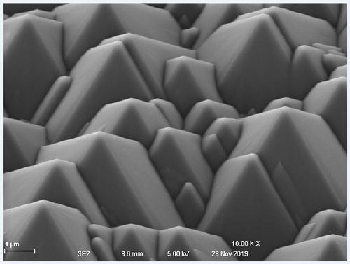
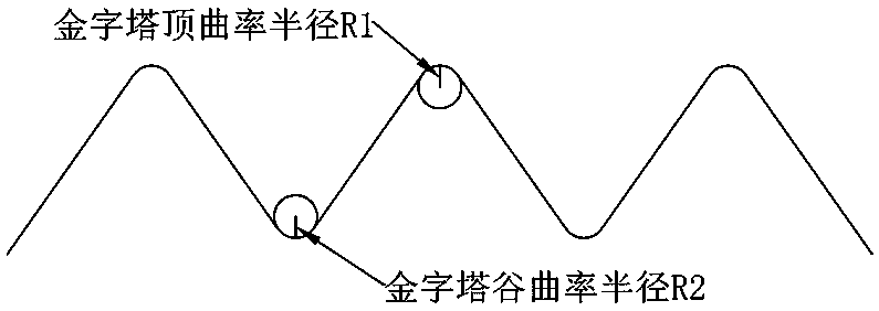
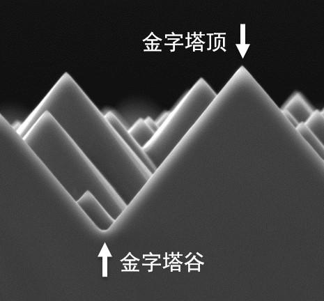
Monocrystalline silicon wafer with rounded pyramid structure and preparation method
A technology of pyramid structure, single crystal silicon wafer, applied in the direction of final product manufacturing, sustainable manufacturing/processing, photovoltaic power generation, etc., can solve the problem that the pyramid top and tower valley are smooth, affect the passivation effect, and the sharp position is difficult to cover the non-contact surface. Crystal silicon passivation layer and other problems, to achieve the effect of reducing the density of defect states, improving passivation quality and minority carrier lifetime, and high cell conversion efficiency
- Summary
- Abstract
- Description
- Claims
- Application Information
AI Technical Summary
Problems solved by technology
Method used
Image

Examples
Embodiment 1
[0043] Embodiment 1 is to carry out nitric acid CP first, then carry out ozone CP, and concrete steps are as follows:
[0044] Step 1: Pre-cleaning, cleaning the silicon wafer in a mixed solution of hydrogen peroxide and KOH, the mass fraction of KOH is 1%, the mass fraction of hydrogen peroxide is 3%, the temperature is 65°C, and the time is 5min. After pre-cleaning, in pure water Rinse silicon wafer for 3 minutes;
[0045] Step 2: Texturing, the mass fraction of KOH in the texturing solution is 7%, and the texturing additive is an additive from Hayashi Pure HPC Company in Japan, and the ratio of the additive to pure water is TT72C13:TK81:DIW=1:7.5:18.4. Put the silicon wafer treated in step 1 into the texturing solution for texturing at a temperature of 85° C. for 15 minutes, and rinse the silicon wafer in pure water for 3 minutes after texturing;
[0046] Step 3: SC1 cleaning, cleaning the silicon wafer in a mixed solution of hydrogen peroxide and KOH, the mass fraction of...
Embodiment 2
[0053] Embodiment 2 is to carry out ozone CP first, then carry out nitric acid CP, and concrete steps are as follows:
[0054] Step 1: Pre-cleaning, cleaning the silicon wafer in a mixed solution of hydrogen peroxide and KOH, the mass fraction of KOH is 1%, the mass fraction of hydrogen peroxide is 3%, the temperature is 65°C, and the time is 5min. After pre-cleaning, in pure water Rinse silicon wafer for 3 minutes;
[0055] Step 2: Texturing, the mass fraction of KOH in the texturing solution is 7%, and the texturing additive is an additive from Hayashi Pure HPC Company in Japan, and the ratio of the additive to pure water is TT72C13:TK81:DIW=1:7.5:18.4. Put the silicon wafer treated in step 1 into the texturing solution for texturing at a temperature of 85° C. for 15 minutes, and rinse the silicon wafer in pure water for 3 minutes after texturing;
[0056] Step 3: SC1 cleaning, cleaning the silicon wafer in a mixed solution of hydrogen peroxide and KOH, the mass fraction of...
Embodiment 3
[0063] Embodiment 3 is to carry out ozone CP and nitric acid CP simultaneously, and concrete steps are as follows:
[0064] Step 1: Pre-cleaning, cleaning the silicon wafer in a mixed solution of hydrogen peroxide and KOH, the mass fraction of KOH is 1%, the mass fraction of hydrogen peroxide is 3%, the temperature is 65°C, and the time is 5min. After pre-cleaning, in pure water Rinse silicon wafer for 3 minutes;
[0065] Step 2: Texturing, the mass fraction of KOH in the texturing solution is 7%, and the texturing additive is an additive from Hayashi Pure HPC Company in Japan, and the ratio of the additive to pure water is TT72C13:TK81:DIW=1:7.5:18.4. Put the silicon wafer treated in step 1 into the texturing solution for texturing at a temperature of 85° C. for 15 minutes, and rinse the silicon wafer in pure water for 3 minutes after texturing;
[0066] Step 3: SC1 cleaning, cleaning the silicon wafer in a mixed solution of hydrogen peroxide and KOH, the mass fraction of KO...
PUM
| Property | Measurement | Unit |
|---|---|---|
| quality score | aaaaa | aaaaa |
| quality score | aaaaa | aaaaa |
| reflectance | aaaaa | aaaaa |
Abstract
Description
Claims
Application Information