Microbolometer and preparation method thereof

A technology of microbolometer and nanowire array, which is applied in the field of microbolometer and its preparation, can solve the problems of large thermal conductivity of devices, poor chemical stability, and inability to obtain detection performance, so as to reduce heat conduction and improve detection with the effect of reading

Active Publication Date: 2020-07-24
NANJING UNIV
View PDF13 Cites 0 Cited by
  • Summary
  • Abstract
  • Description
  • Claims
  • Application Information

AI Technical Summary

Problems solved by technology

CN101774530B discloses a microbolometer and its preparation method. The heat-sensitive material used in the patent and the infrared absorbing layer are carbon nanotube-amorphous silicon composite films, which can effectively improve the low and low conductivity of traditional amorphous silicon thermistor films. The disadvantage of poor chemical stability, while avoiding the negative impact of the traditional doping process on the amorphous silicon film
However, the structure adopted by the above two patents is still the traditional way of laying the entire microbridge directly on the cavity structure with the readout circuit substrate, so that the entire device still has a large thermal conductivity, resulting in the smallest detectable Temperature will also be heavily discounted for excellent detection performance

Method used


Image

  • Microbolometer and preparation method thereof
  • Microbolometer and preparation method thereof
  • Microbolometer and preparation method thereof

Examples


Embodiment Construction

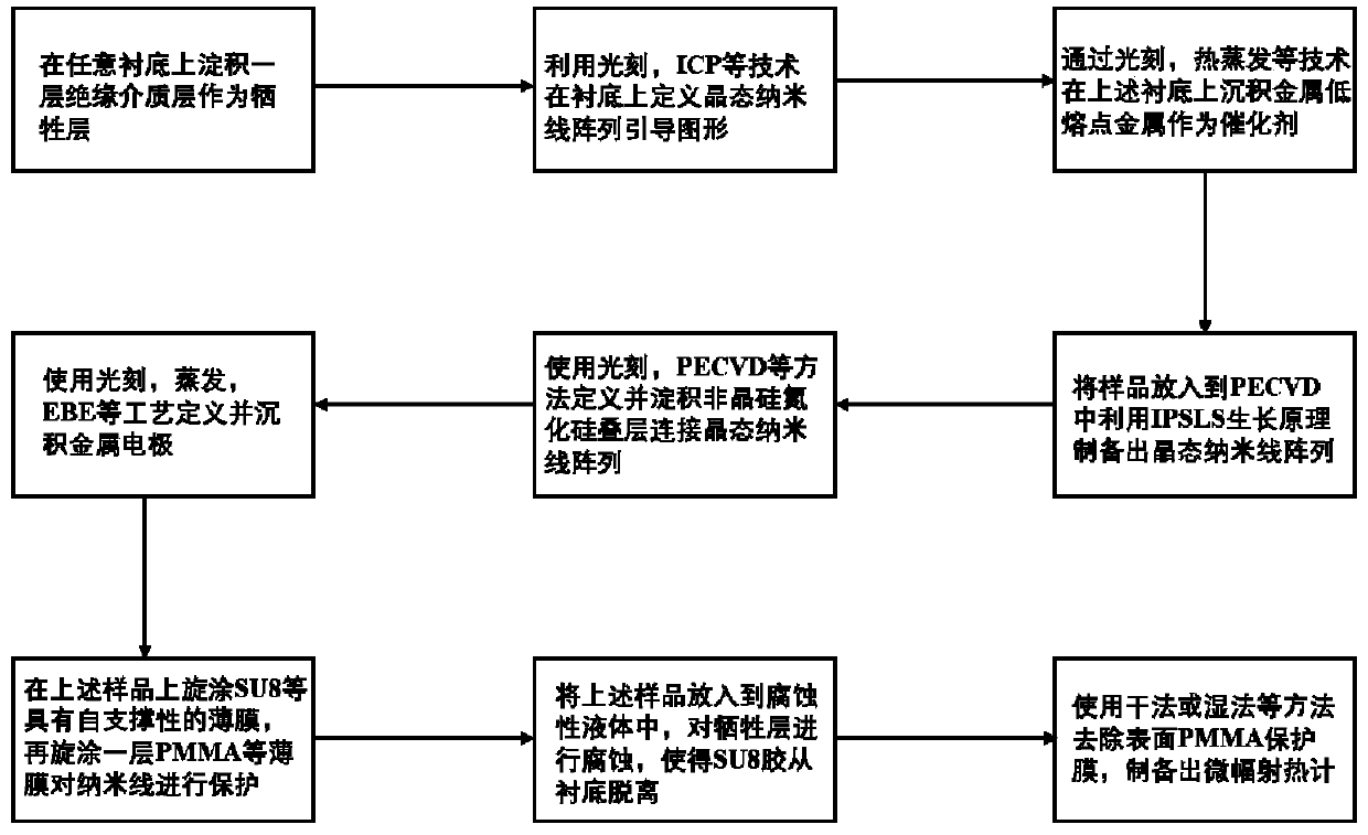
[0031] The present invention will be further explained below in conjunction with the accompanying drawings and specific embodiments.

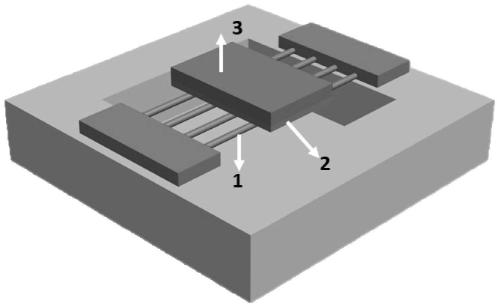
[0032] Such as Figure 2-3 As shown, this embodiment discloses a microbolometer, which includes a horizontally distributed planar semiconductor crystalline nanowire array 1 and amorphous silicon layered sequentially above the planar semiconductor crystalline nanowire array from bottom to top. Layer 2 and Silicon Nitride Layer 3.

[0033] Both ends of the planar semiconductor crystalline nanowires are provided with metal electrodes. Its metal electrodes can be PT (12nm)-AL (80nm) system, Ti-Au system, Ni and other metal materials, and the metal contact can be improved by rapid thermal annealing process. The evaporation method may use a thermal evaporation system, a magnetron sputtering system, or an electron beam evaporation system.

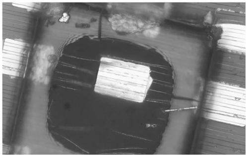
[0034] Also disclosed in this embodiment is a preparation method for a microbolometer, such as figure 1 As s...


PUM

PropertyMeasurementUnit
diameteraaaaaaaaaa
thicknessaaaaaaaaaa
diameteraaaaaaaaaa

Abstract

The invention discloses a microbolometer which comprises a horizontally distributed planar semiconductor crystalline nanowire array, and an amorphous silicon layer and a silicon nitride layer which are sequentially laminated on the planar semiconductor crystalline nanowire array from bottom to top, wherein metal electrodes are arranged at the two ends of the planar semiconductor crystalline nanowire array. The structure of a common microbolometer device at present is changed, a suspended crystalline nanowire is used as a support, the suspended amorphous silicon (sensitive layer) silicon nitride (photosensitive layer) has the advantages that due to the limitation of the surface of the suspended crystalline nanowire on heat conduction, the detection island area can be well thermally insulated, and the nanowire has lower resistivity and can also be used as a conductive channel so that the conversion from the thermal performance to the electrical performance of the device is greatly improved.

Description

technical field [0001] The present invention relates to a microbolometer and a preparation method thereof, more specifically to a method for connecting and suspending amorphous silicon nitride laminated films by using a programmable crystalline nanowire array, especially involving the use of suspending Confinement of thermal conduction by the surface of nanowires, and the high thermal resistivity of amorphous silicon for the fabrication of novel microbolometer devices. Background technique [0002] Infrared spectrum can be divided into near-infrared (wavelength range 0.75 μm ~ 2.5 μm), mid-infrared (wavelength range 2.5 μm ~ 25 μm) and far infrared (wavelength range 25 μm ~ 300 μm) according to its relationship with visible light. Infrared spectroscopy has a wide range of applicability to samples. Solid, liquid or gaseous samples can be used, and inorganic, organic and polymer compounds can be detected; It is also widely used in astronomy, meteorology, remote sensing, biolo...

Claims


Application Information

Patent Timeline
Patent Type & Authority Applications(China)
IPC IPC(8): B82B1/00B82B3/00G01J5/20B82Y15/00B82Y40/00
CPCB82B1/00B82B3/0014B82Y15/00B82Y40/00G01J5/20G01J2005/204G01J2005/206
Inventor 余林蔚孙莹董泰阁王军转
Owner NANJING UNIV
Why Eureka
Try Eureka