Silicon negative pole piece, production method and application thereof
A silicon negative electrode and negative electrode technology, applied in the direction of negative electrode, electrode manufacturing, electrode rolling/calendering, etc., can solve the problems of unfavorable batch production, long-term commercial application, and complicated modification methods, so as to improve production efficiency and enhance Toughness, the effect of reducing the aging time
- Summary
- Abstract
- Description
- Claims
- Application Information
AI Technical Summary
Problems solved by technology
Method used
Image
Examples
preparation example Construction
[0057] The preparation method of the present invention will be further described in detail in conjunction with specific examples below. It should be understood that the following examples are only for illustrating and explaining the present invention, and should not be construed as limiting the protection scope of the present invention. All technologies realized based on the above contents of the present invention are covered within the scope of protection intended by the present invention.
[0058] The experimental methods used in the following examples are conventional methods unless otherwise specified; the reagents and materials used in the following examples can be obtained from commercial sources unless otherwise specified.
Embodiment 1
[0060] Weigh 80g of nano-silicon material, 0.5g of binder PAA, 0.5g of dispersant sodium dodecylbenzenesulfonate, 2g of conductive agent carbon nanotubes, 2g of thickener CMC, and 100g of water.
[0061] First add the thickener to half of the formula amount of water, then add the binder, dispersant, conductive agent and negative electrode active material in sequence under stirring conditions, and add the remaining water after the dispersion is uniform; grind the obtained slurry, After sieving, negative electrode slurry is obtained.
[0062] The negative electrode slurry is coated on the surface of the copper current collector, and the thickness of the active material layer obtained after coating and rolling is 100±0.5 μm.
[0063] Then 2g of graphite fiber, 1g of nickel fiber and 10g of PVDF glue were stirred and mixed evenly, and the prepared glue was spin-coated on the rolled active material layer using a rotary glue coater, and after vacuum drying, it was mixed with electro...
Embodiment 2-17
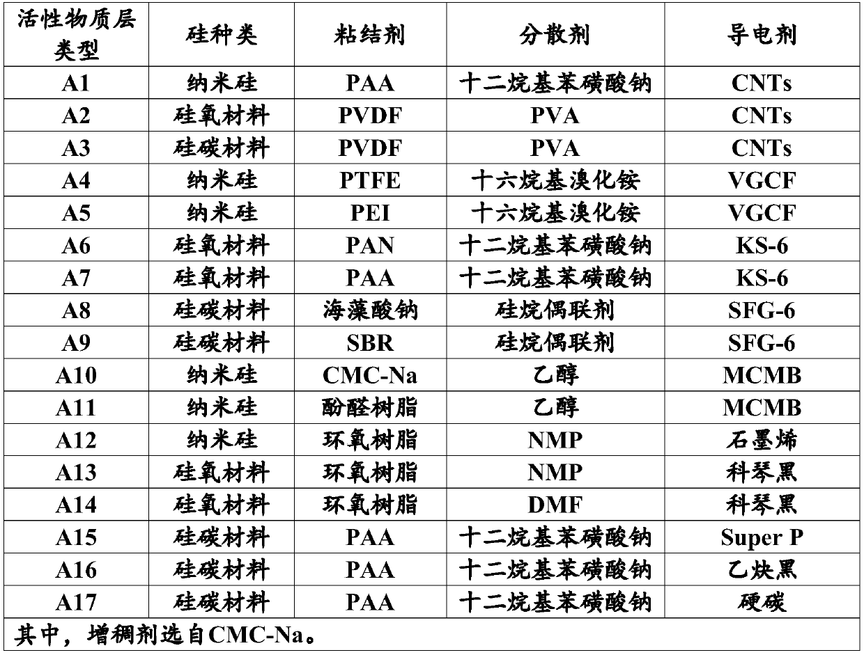
[0066] The preparation method is the same as in Example 1, the only difference is that in the preparation process of the silicon negative plate, the selection and dosage of each component in the active material layer are different, and the selection and dosage of each component in the functional layer are different, as shown in Table 1-Table 5.
[0067] Table 1 is the selection of each component in the active material layer described in embodiment 1-17
[0068]
[0069] Table 2 is the selection of each component in the functional layer described in embodiment 1-17
[0070] Functional layer type carbon fiber metal fiber Conductive plastic B1 Graphite Carbon Fiber nickel fiber PVDF B2 Graphite Carbon Fiber aluminum fiber PVDF B3 carbon nanotube fiber zinc fiber PAAA B4 carbon nanotube fiber copper fiber PAAA B5 graphene fiber iron fiber PAN B6 graphene fiber manganese fiber PAN B7 carbon fiber ...
PUM
| Property | Measurement | Unit |
|---|---|---|
| thickness | aaaaa | aaaaa |
| thickness | aaaaa | aaaaa |
| electrical resistivity | aaaaa | aaaaa |
Abstract
Description
Claims
Application Information


