Epitaxy method for growing blue light emitting diode on m-plane gallium nitride substrate

A gallium nitride substrate and light-emitting diode technology, applied in chemical instruments and methods, crystal growth, single crystal growth, etc., can solve the problems of growing GaN thin films and InGaN quantum well In incorporation difficulties

Active Publication Date: 2020-08-11
ANHUI UNIVERSITY OF TRADITIONAL CHINESE MEDICINE
View PDF5 Cites 1 Cited by
  • Summary
  • Abstract
  • Description
  • Claims
  • Application Information

AI Technical Summary

Problems solved by technology

[0003] The purpose of the present invention is to overcome the deficiencies in the prior art, and provides an epitaxial method for growing blue light-emitting diodes on an M-face gallium nitride substrate, so as to solve the problem of growing GaN thin films and InGaN quantum wells on an M-face GaN substrate in the prior art. Incorporate more difficult technical problems

Method used


Image

  • Epitaxy method for growing blue light emitting diode on m-plane gallium nitride substrate
  • Epitaxy method for growing blue light emitting diode on m-plane gallium nitride substrate
  • Epitaxy method for growing blue light emitting diode on m-plane gallium nitride substrate

Examples


Embodiment

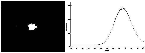
[0034] refer to Figure 1-5 , this embodiment provides a method for growing blue light-emitting diodes on an m-plane gallium nitride substrate, wherein the m-plane gallium nitride substrate is a non-polar self-supporting m-plane with a size of 5mm*10mm and no off-angle prepared by the HVPE method GaN commercial products

[0035] For product specification parameters, please refer to "http: / / shop.nanowin.com.cn / product_center.php".

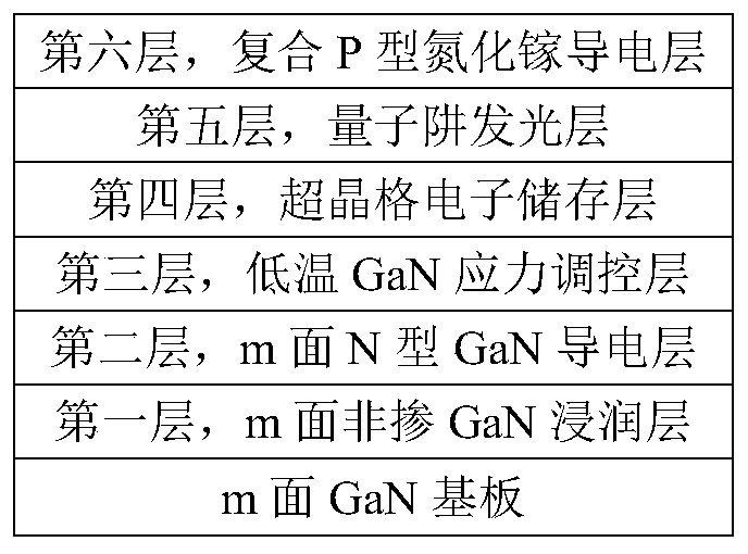
[0036] The structure of the present invention is as figure 1 ,include:

[0037] S1. Provide an m-plane GaN substrate;

[0038] S2, growing a non-doped GaN homoepitaxial thin film wetting layer on the substrate by metal organic chemical vapor deposition;

[0039] S3. Growing an N-type conductive GaN epitaxial layer on the non-doped GaN thin film at high temperature by metal-organic chemical vapor deposition;

[0040] S4. Growing a gallium nitride stress regulating layer on the N-conductive GaN thin film by metal-organic chemical vapor deposition...

specific Embodiment

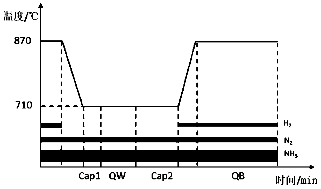
[0045] 1) Put the m-plane self-supporting GaN template into the metal organic chemical vapor deposition (MOCVD) equipment.

[0046] 2) In order to suppress the decomposition of the GaN surface as the temperature increases, the GaN template is 2 / NH 3 Slowly heat up to 950°C under atmosphere, N 2 / NH 3 The total air flow is controlled at 120-150slm / min, where NH 3 The proportion is 40%-50%, the reaction chamber pressure is 75torr, and the heating rate is 60-80℃ / min.

[0047] 3) Keep the temperature at 950°C and the pressure in the reaction chamber at 75torr, reduce the amount of N2 feeding, and start feeding H 2 , control N 2 :H 2 :NH 3 The ratio is 25:25:50, the total air flow is 120-150slm / min, and the step time is 30s.

[0048] 4) Keep the above growth conditions unchanged, pass through trimethylgallium TMGa to provide Ga source, and start to grow the GaN wetting layer, the growth rate is controlled at 15-20nm / min, and the growth thickness is 200nm.

[0049] 5) Rais...


PUM

PropertyMeasurementUnit
thicknessaaaaaaaaaa
emission peakaaaaaaaaaa
thicknessaaaaaaaaaa

Abstract

The invention discloses an epitaxy method for growing a blue light emitting diode on an m-plane gallium nitride substrate. The invention relates to the technical field of semiconductor epitaxial layergrowth. The method comprises the following steps of: growing a non-doped gallium nitride homogeneous epitaxial film infiltration layer at the top of an m-plane GaN substrate by using a metal organicchemical vapor deposition method; sequentially generating an N-type conductive GaN epitaxial layer, a GaN stress regulation and control layer, a GaN / InGaN superlattice electron storage layer, an InGaN / GaN multi-quantum well light-emitting epitaxial layer and a composite P-type GaN layer from bottom to top by using a metal organic chemical vapor deposition method; according to the invention, m-plane homoepitaxy is realized to obtain a flat surface, and effective incorporation of In in the InGaN layer is realized to realize blue light quantum well excitation.

Description

technical field [0001] The invention relates to the technical field of growing semiconductor epitaxial layers, in particular to an epitaxial method for growing a blue light-emitting diode on an m-plane gallium nitride substrate. Background technique [0002] Gallium Nitride (GaN), as a third-generation semiconductor material, has direct band gap, large band gap, strong breakdown field, high electron drift saturation velocity, high thermal conductivity, small dielectric constant, high hardness, and stable chemical properties And anti-radiation, high temperature and other advantages. It has huge application potential and wide market in the fields of blue, green and purple light-emitting diodes, laser diodes, ultraviolet detectors and radiation-resistant, high-frequency, high-temperature, high-voltage and other electronic devices. At present, GaN thin films are mainly grown on GaN (0001) plane (c plane) films along the polar axis c direction on sapphire and silicon carbide sub...

Claims


Application Information

Patent Timeline
Patent Type & Authority Applications(China)
IPC IPC(8): H01L33/00H01L21/02H01L33/06H01L33/32C30B25/16C30B29/40
CPCC30B25/16C30B29/406H01L21/02389H01L21/02433H01L21/02458H01L21/0254H01L21/0262H01L33/0075H01L33/06H01L33/32
Inventor 刘园旭
Owner ANHUI UNIVERSITY OF TRADITIONAL CHINESE MEDICINE
Why Eureka
Try Eureka