
Method for preparing monocrystalline silicon film and silicon P-N junction through high-temperature fused salt electro-deposition

A technology of high-temperature molten salt and electrodeposition, applied in the field of semiconductors, to achieve the effects of improving production efficiency, reducing production energy consumption, and simple operation process

Pending Publication Date: 2020-08-25
SHANGHAI UNIV
View PDF3 Cites 1 Cited by
  • Summary
  • Abstract
  • Description
  • Claims
  • Application Information

AI Technical Summary

Problems solved by technology

However, this method has strict requirements on corrosion time and solution system quality control.

Method used


Image

  • Method for preparing monocrystalline silicon film and silicon P-N junction through high-temperature fused salt electro-deposition
  • Method for preparing monocrystalline silicon film and silicon P-N junction through high-temperature fused salt electro-deposition
  • Method for preparing monocrystalline silicon film and silicon P-N junction through high-temperature fused salt electro-deposition

Examples


Embodiment 1

[0042] In this embodiment, the specific operation steps are as follows:

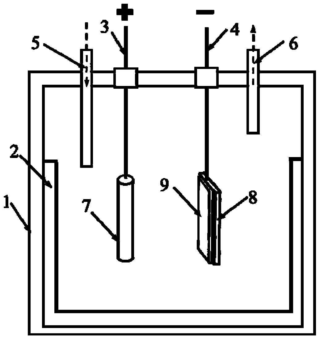
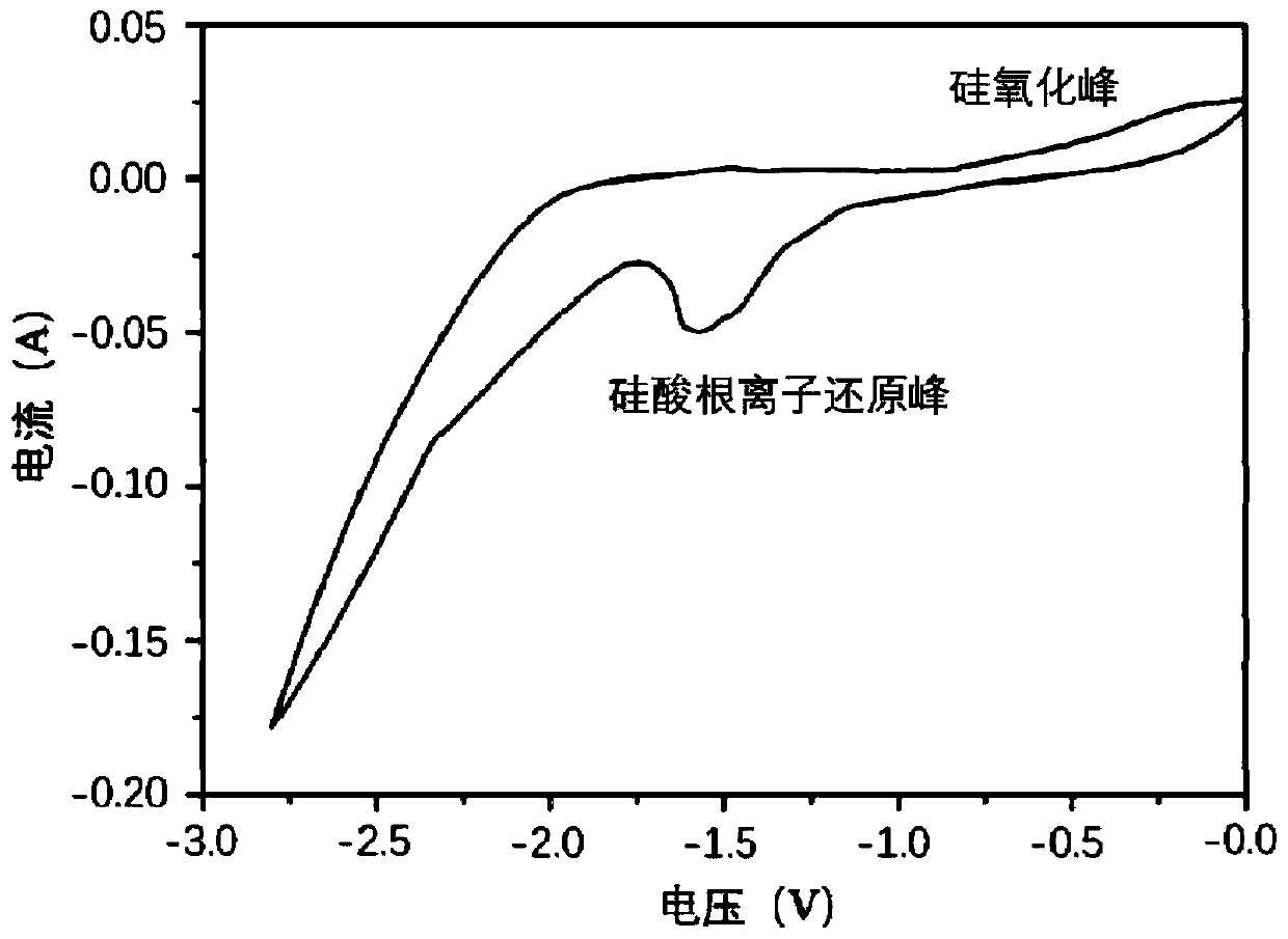
[0043] (75g) CaCl 2 -(2.0g)SiO2 2 - (2.0 g) CaO raw material was added into a high-purity quartz crucible, and the temperature was raised to 500° C. under a high-purity argon atmosphere, and kept for 24 hours. Then it was heated to 850°C under high-purity argon atmosphere and kept for 48h. Two high-purity graphite rods were used as anode and cathode, and put into a crucible for pre-electrolysis. The pre-electrolysis voltage was 2.5V and the time was 12h. After the pre-electrolysis, a high-purity graphite rod was put in again as the anode of the electrolytic cell, and the P-type monocrystalline silicon wafer [100] was used as the cathode of the electrolytic cell, that is, the substrate of the product, for electrodeposition, and the obtained cyclic voltammetry curve was as follows figure 2 shown. This example uses Ca 3 (PO 4 ) 2 as a source of doping elements. This time the current density was 15m...

Embodiment 2

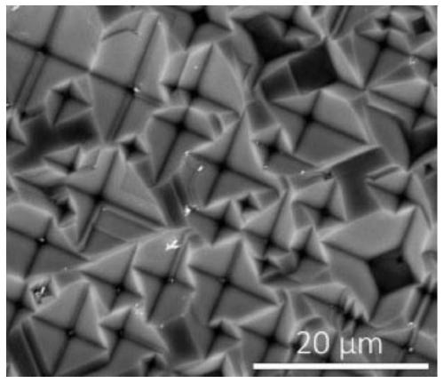
[0045] The implementation of this case is roughly the same as Example 1, but the electrodeposition time is 1h, and the surface morphology of the obtained product is as follows Figure 5 As shown, the cross-section Figure 6 shown. It can be seen that the surface of the epitaxially grown silicon film is still composed of inverted pyramids, and the thickness of the deposited single crystal silicon film is about 3 μm.

Embodiment 3

[0047] (75g) CaCl 2 -(1.8g) SiO2 2 - (1.6g) CaO raw material was added into a high-purity quartz crucible, and the temperature was raised to 500° C. under a high-purity argon atmosphere, and kept for 24 hours. Then it was heated to 850°C under high-purity argon atmosphere and kept for 48h. Two high-purity graphite rods were used as anode and cathode, and put into a crucible for pre-electrolysis. The pre-electrolysis voltage was 2.5V and the time was 12h. Then perform intermittent pre-electrolysis three times. During electrodeposition, a high-purity graphite rod was placed again as the anode of the electrolytic cell, and the P-type monocrystalline silicon wafer in the [100] direction was used as the cathode of the electrolytic cell, that is, the substrate of the product. This time, Ca was used for doping. 3 (PO 4 ) 2 As a source of doping elements, a small amount of Ca is added to the electrolytic cell 3 (PO 4 ) 2 , and applied a constant voltage of 2.4V for continuous ...


PUM

PropertyMeasurementUnit
thicknessaaaaaaaaaa
thicknessaaaaaaaaaa

Abstract

The invention discloses a method for preparing a monocrystalline silicon film and a silicon P-N junction through high-temperature fused salt electro-deposition, and relates to the technical field of semiconductors. According to the method, a CaCl2-SiO2-CaO system or a CaCl2-CaSiO3 system can be selected as a raw material, a doping agent is added, and under the conditions of constant current, constant voltage or pulse current, inert gas atmosphere and 850 DEG C, the monocrystalline silicon film material is epitaxially grown on a monocrystalline substrate through electro-deposition. The operation method is simple, an inverted pyramid surface structure is achieved while P-P type, P-N junction type and N-N type monocrystalline silicon film materials are prepared, surface light absorption can be effectively enhanced, and the conversion efficiency of a solar cell is improved. The thickness of the monocrystalline silicon film material can be accurately regulated and controlled by changing current parameters, voltage parameters, time and the like, continuous preparation can be realized by periodically supplementing raw materials, the preparation efficiency is improved, and the method has the advantages of short process, low energy consumption and the like.

Description

technical field [0001] The invention relates to the technical field of semiconductors, in particular to a method for preparing a single crystal silicon film and a silicon P-N junction by high-temperature molten salt electrodeposition. Background technique [0002] Facing the depletion of fossil energy and its pollution to the environment, it is particularly important to explore, develop and utilize sustainable new energy. The use of solar photovoltaic cells to generate electricity is a new, renewable and clean energy source, so it has attracted widespread attention. Among all these materials that can generate photovoltaic power generation, P-N junction photovoltaic cells made of single crystal silicon are currently the most widely used, and in the foreseeable future, silicon-based photovoltaic technology will still be the mainstream technology in the field of photovoltaics. At present, the methods for preparing P-N junction single crystal silicon include diffusion method, i...

Claims


Application Information

Patent Timeline
Patent Type & Authority Applications(China)
IPC IPC(8): C30B9/14C25D9/08C25D7/12C30B29/06
CPCC30B9/14C25D9/08C25D7/12C30B29/06
Inventor 邹星礼唐蔚庞忠亚李想汪淑娟卢明辉许茜鲁雄刚
Owner SHANGHAI UNIV
Learn More