A kind of preparation method of ferroelectric single crystal thin film for infrared focal plane device
An infrared focal plane, ferroelectric single crystal technology, which is applied to semiconductor devices, circuits, electrical components, etc., can solve the problems of difficulty in preparing two-dimensional focal plane array devices, lithium tantalate single crystal thin films, and material waste. , to reduce costs, protect integrity and quality, and protect integrity
- Summary
- Abstract
- Description
- Claims
- Application Information
AI Technical Summary
Problems solved by technology
Method used
Image
Examples
preparation example Construction
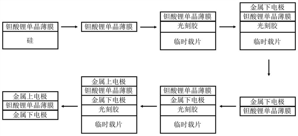
[0039] The invention proposes a method for preparing a ferroelectric single crystal thin film for infrared focal plane devices, with figure 1 The preparation process of the ferroelectric single crystal thin film is described, and the specific steps are as follows:
[0040] (1) Sample preparation: cut silicon-based lithium tantalate single crystal film into 0.5cm×0.5cm or 1.0cm×1.0cm size, wash with deionized water, and blow dry with nitrogen.
[0041] (2) Obtaining a self-supporting lithium tantalate film: place a silicon-based lithium tantalate wafer in a 10% tetramethylammonium hydroxide solution, heat it in a water bath to 75-85° C., and continue for 12-24 hours. After the silicon is completely corroded, the lithium tantalate film is taken out and placed in absolute alcohol, and then the lithium tantalate film is taken out with a Mylar film and dried naturally.
[0042] (3) Fix lithium tantalate on the temporary carrier: Spin-coat photoresist on the temporary carrier, the ...
Embodiment
[0049] (1) Cut the silicon-based lithium tantalate single crystal film into a size of 1.0 cm×1.0 cm, wash it with deionized water, and dry it with nitrogen gas.
[0050] (2) Place the silicon-based lithium tantalate wafer in a 10% tetramethylammonium hydroxide solution, heat it in a water bath to 80°C, and continue for 24 hours. After the silicon is completely corroded, take out the lithium tantalate film and place it In anhydrous alcohol, then remove the lithium tantalate film with Mylar film and let it dry naturally.
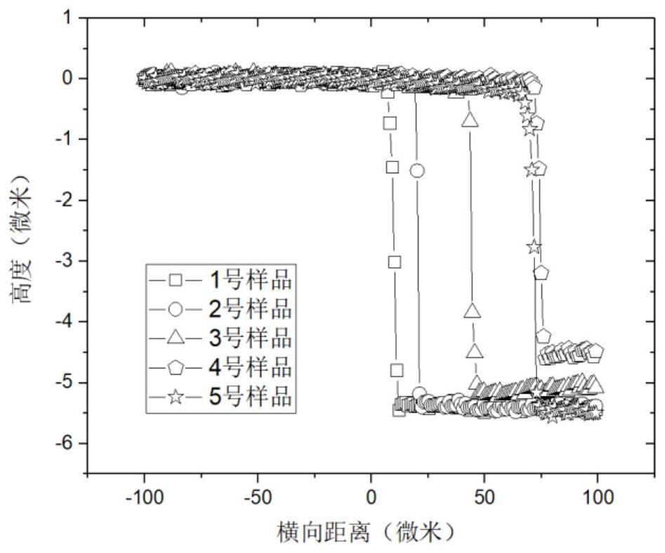
[0051] (3) Test the thickness of the lithium tantalate film on the Mylar film with a step meter, and test 5 different samples respectively. The test results are as follows image 3 As shown, the average thickness is about 5.14 μm.
[0052] (4) Spin-coat photoresist on the silicon wafer, the photoresist model is AZ5214, the rotating speed is 1000 rpm, spin-coat for 40 seconds, then place the silicon wafer with the photoresist in absolute alcohol, use Mylar Me...
PUM
| Property | Measurement | Unit |
|---|---|---|
| thickness | aaaaa | aaaaa |
| thickness | aaaaa | aaaaa |
| thickness | aaaaa | aaaaa |
Abstract
Description
Claims
Application Information


