Gallium oxide wafer surface treatment method

A surface treatment, gallium oxide technology, applied in chemical instruments and methods, post-treatment, post-treatment details, etc., can solve the problems of low corrosion removal rate, high corrosion temperature, long corrosion time, etc., and achieve high corrosion efficiency and corrosion temperature. Low, internal stress relief effect

Active Publication Date: 2022-04-01
杭州镓仁半导体有限公司
View PDF5 Cites 0 Cited by
  • Summary
  • Abstract
  • Description
  • Claims
  • Application Information

AI Technical Summary

Problems solved by technology

[0005] In order to solve the problems in the existing corrosion technology of gallium oxide single crystal materials, the corrosion removal rate is lower than 100nm / h, the corrosion time is long, the efficiency is low, and the corrosion temperature is high. The present invention provides a surface treatment method for gallium oxide wafers. The processing method invented is to remove the damaged layer of the wafer caused by the machining process, dry etching process, etc., eliminate the internal stress of the wafer, and produce a uniform wafer that meets the roughness requirements of the subsequent process. The processing method of the present invention has a low corrosion temperature, High corrosion efficiency and good process control performance

Method used


Image

  • Gallium oxide wafer surface treatment method
  • Gallium oxide wafer surface treatment method

Examples


Embodiment 1

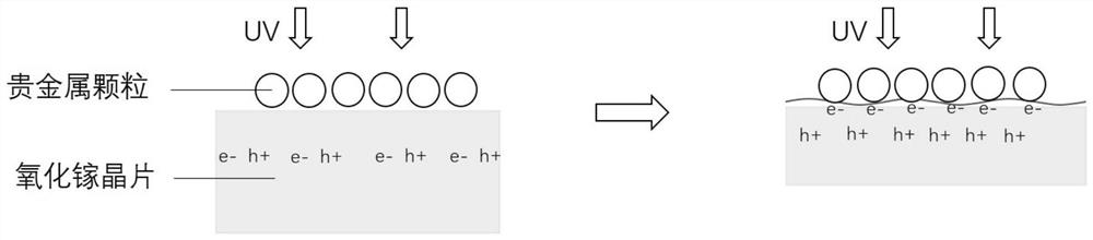
[0047] This embodiment provides a gallium oxide wafer surface treatment method, including:

[0048] 1) After the gallium oxide wafer is cleaned to remove organic matter and metal particles on the surface, it is blown dry with nitrogen;

[0049] 2) Put the gallium oxide wafer into the mixed solution of silver nitrate and hydrofluoric acid for 60s to deposit a certain amount of Ag particles; after the silver plating is finished, wash it with deionized water and enter the next metal-assisted corrosion process;

[0050] 3) Each component of the corrosion solution is hydrofluoric acid 12wt.%, the oxidant is sodium persulfate 0.005wt.%, the surfactant is ethanol 0.02wt.%. The wafer is irradiated, and the distance between the light source and the wafer is 6cm;

[0051] 4) Put the gallium oxide wafer after etching into concentrated nitric acid solution and let it stand for 0.5 h; finally, take out the wafer from which the metal particles have been removed, rinse it with deionized wat...

Embodiment 2

[0054] This embodiment provides a gallium oxide wafer surface treatment method, including:

[0055] 1) After the gallium oxide wafer is cleaned to remove organic matter and metal particles on the surface, it is blown dry with nitrogen;

[0056] 2) Deposit Au particles with a thickness of 2-5nm on the surface of the cleaned wafer by vacuum evaporation; after the gold spraying is completed, enter the next step of metal-assisted corrosion process;

[0057] 3) Each component of the corrosion solution is hydrofluoric acid 12wt.%, the oxidant is sodium persulfate 0.005wt.%, the surfactant is ethanol 0.02wt.%. The wafer is irradiated, and the distance between the light source and the wafer is 6cm;

[0058] 4) Put the gallium oxide wafer after etching into the aqua regia solution and let it stand for 1 hour; finally, take out the wafer from which the metal particles have been removed, rinse it with deionized water, and dry it with nitrogen gas.

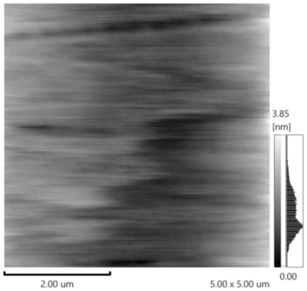
[0059] At room temperature, the corr...

Embodiment 3

[0061] This embodiment provides a gallium oxide wafer surface treatment method, including:

[0062] 1) After the gallium oxide wafer is cleaned to remove organic matter and metal particles on the surface, it is blown dry with nitrogen;

[0063] 2) Put the wafer into the mixed solution of silver nitrate and hydrofluoric acid for 60s to deposit a certain amount of Ag particles; after the silver plating is finished, rinse with deionized water and enter the next metal-assisted corrosion process;

[0064] 3) Each component of the corrosion solution is 12wt.% of hydrofluoric acid, 15wt.% of hydrogen peroxide as the oxidizing agent, 0.02wt.% of ethanol as the surfactant, and the ultraviolet lamp with a power of 120W and a wavelength of 254nm is used for the corrosion of the corrosive liquid. The wafer is irradiated, and the distance between the light source and the wafer is 6cm;

[0065] 4) Put the gallium oxide wafer after etching into concentrated nitric acid solution and let it s...


PUM


Abstract

The invention provides a gallium oxide wafer surface treatment method, which comprises the following steps of: using noble metal particles as a catalyst and a mixed solution of hydrofluoric acid, an oxidizing agent and a surfactant as a corrosive agent at room temperature through a noble metal auxiliary corrosion method, so that the surface of a gallium oxide wafer can be quickly dissolved by the corrosive agent; precious metal particles are subjected to local primary battery reaction on the surface of a gallium oxide wafer, the work function of precious metal is higher, when the precious metal is in contact with the surface of gallium oxide, a certain electric field exists in a space charge area, energy band bending is caused, potential difference exists between the surface and the interior of a semiconductor, and electrons are extracted from the crystal by a precious metal catalyst. Especially under the irradiation of an ultraviolet lamp, the formation of electrons and hole pairs on the surface of gallium oxide is accelerated, and the possibility of compounding of photo-induced electron and hole pairs is reduced by the escape of electrons, so that the hole accumulation region on the surface of gallium oxide is promoted to generate an oxidation reaction, oxygen is generated, an oxidizing agent in a solution is reduced, Ga ions are dissolved in hydrofluoric acid, and the corrosion process is completed. According to the processing method, the wafer damage layer caused by the machining process, the dry etching process and the like can be removed, the internal stress of the wafer is eliminated, and the uniform wafer meeting the roughness requirement of the subsequent process is manufactured.

Description

technical field [0001] The invention belongs to the technical field of semiconductor wafer manufacturing, and relates to a gallium oxide wafer, in particular to a gallium oxide wafer surface treatment method with low corrosion temperature, high corrosion efficiency, controllable corrosion rate and good stability. Background technique [0002] As a new generation of ultra-wide bandgap semiconductor material, gallium oxide has a bandgap width of 4.7-4.9eV, high breakdown electric field strength, large transmission range, high Baliga quality factor, low device power consumption, and stable physical and chemical properties. It has great application value in the fields of high-voltage and high-power electronic devices and solar-blind ultraviolet photoelectric devices, and is an important supplement to the third-generation wide-bandgap semiconductor materials represented by SiC and GaN. Gallium oxide has found six crystal phases and multiple crystal structures, and the consistent ...

Claims


Application Information

Patent Timeline
Patent Type & Authority Applications(China)
IPC IPC(8): C30B33/10C30B29/16H01L21/02
Inventor 张辉刘莹莹金竹夏宁马可可杨德仁
Owner 杭州镓仁半导体有限公司
Why Eureka
Try Eureka