Preparation method of stable and high-efficiency silicon heterojunction solar cell
A silicon heterojunction, solar cell technology, applied in circuits, electrical components, photovoltaic power generation and other directions, can solve the problems of solar cell photoelectric conversion performance decline, production capacity decline, cost rise, etc., to improve internal stress, reduce consumption, The effect of prolonging time
- Summary
- Abstract
- Description
- Claims
- Application Information
AI Technical Summary
Problems solved by technology
Method used
Image
Examples
Embodiment 1
[0035] A method for preparing a stable high-efficiency silicon heterojunction solar cell, comprising the following steps:
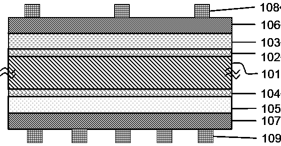
[0036] S1. Texture making and cleaning: Use KOH, NaOH and other alkaline solutions to anisotropically corrode monocrystalline silicon to make texturing of n-type single crystal, and use RCA1 and RCA2 solutions to clean silicon wafers to obtain a crystalline silicon substrate with a clean surface 101;
[0037] S2. Depositing an amorphous silicon thin film passivation layer: sequentially depositing a 5 nm intrinsic amorphous silicon thin film 102 and a 10 nm doped silicon-based thin film passivation layer 103 on the first light-receiving surface on the first surface of the crystalline silicon substrate 101, The doped silicon-based thin-film passivation layer 103 on the first light-receiving surface is an n-type doped amorphous silicon stacked thin film; the intrinsic silicon-based thin-film passivation layers 104 and 15 are successively 5 nm on the second s...
Embodiment 2
[0046] A method for preparing a stable high-efficiency silicon heterojunction solar cell, comprising the following steps:
[0047] S1. Texture making and cleaning: Use KOH, NaOH and other alkali solutions to anisotropically corrode single crystal silicon to make texture on n-type single crystal, and use RCA1 and RCA2 solutions or other oxidation methods to clean the surface of the silicon wafer to obtain a surface Cleaned crystalline silicon substrate 101;
[0048] S2. Depositing an amorphous silicon thin film passivation layer: in the same vacuum chamber, on the first surface of the crystalline silicon substrate 101, sequentially deposit a 5 nm intrinsic amorphous silicon thin film 102 and a 6 nm doping of the first light-receiving surface Silicon-based thin-film passivation layer 103, the doped silicon-based thin-film passivation layer 103 on the first light-receiving surface is an n-type doped amorphous silicon stacked thin film; in the same vacuum chamber, sprinkle flowers...
PUM
| Property | Measurement | Unit |
|---|---|---|
| thickness | aaaaa | aaaaa |
| thickness | aaaaa | aaaaa |
| thickness | aaaaa | aaaaa |
Abstract
Description
Claims
Application Information


