Method for realizing gallium nitride p-type doping based on Mg ion implantation and high-temperature annealing process

A technology of high-temperature annealing and ion implantation, which is applied in the manufacture of electrical components, semiconductor/solid-state devices, circuits, etc., can solve problems such as immaturity, low activation rate, and material surface decomposition, and achieves inhibition of decomposition, low cost, and reduced material damage Effect

Pending Publication Date: 2020-09-01
NANJING UNIV
View PDF6 Cites 5 Cited by
  • Summary
  • Abstract
  • Description
  • Claims
  • Application Information

AI Technical Summary

Problems solved by technology

However, in GaN materials, the technology of p-type doping based on ion implantation is still immature
In the p-type doping of GaN, limited by the low activation rate, a higher doping concentration (>10 19 / cm 3 ) and increase the annealing activation temperature, usually above 1000°C, but this will bring key problems such as material surface decomposition

Method used


Image

  • Method for realizing gallium nitride p-type doping based on Mg ion implantation and high-temperature annealing process
  • Method for realizing gallium nitride p-type doping based on Mg ion implantation and high-temperature annealing process
  • Method for realizing gallium nitride p-type doping based on Mg ion implantation and high-temperature annealing process

Examples


Embodiment 1

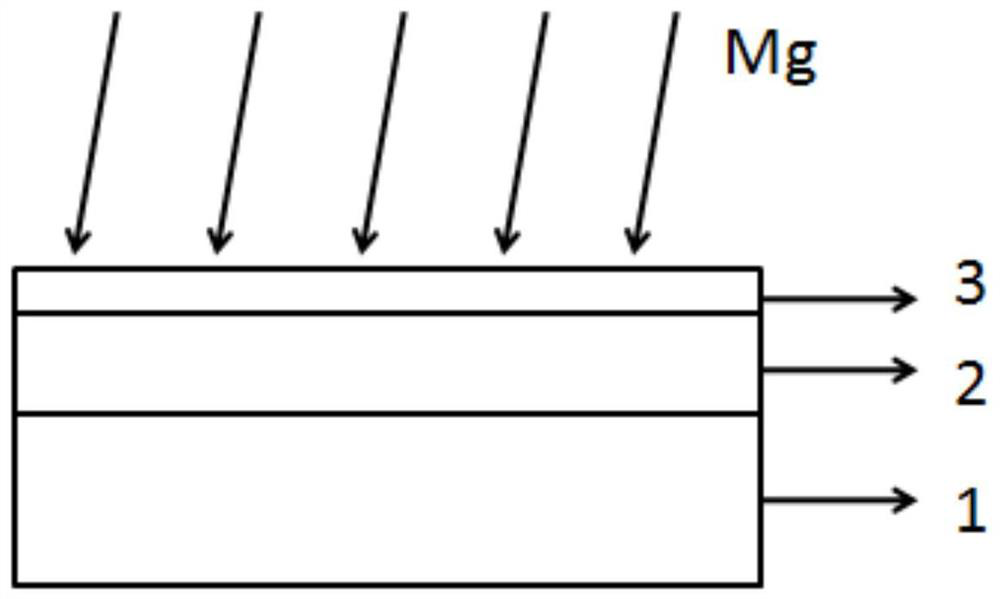
[0035] A method for realizing p-type doping of gallium nitride based on Mg ion implantation and high temperature annealing process, comprising the following steps:

[0036] S1: Deposit 20nm AlN material on the surface of GaN sample,

[0037] S2: Select the appropriate energy and dose of Mg ion implantation for ion implantation. In this embodiment, two-step implantation is selected. The first implantation energy is 30keV, and the dose is 1.5×10 14 cm -2 , the second implantation energy is 60keV, and the dose is 2×10 14 cm -2 ,

[0038] S3: remove AlN material,

[0039] S4: Deposit 200nm silicon dioxide on the surface of the GaN sample as a protective layer during high temperature annealing,

[0040]S5: Perform high-temperature annealing on the GaN sample, the gas atmosphere is a nitrogen atmosphere, the temperature is 1230°C, and the annealing time is 30 minutes.

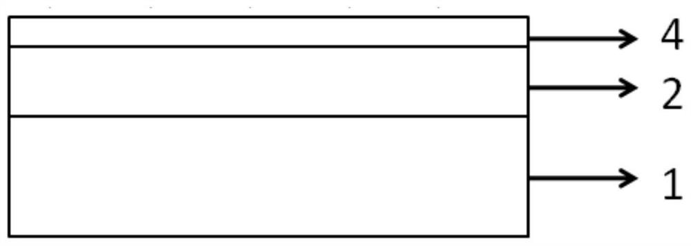
[0041] S6: Remove the silicon dioxide high-temperature annealing protective layer on the GaN surface to obta...

Embodiment 2

[0046] A method for realizing p-type doping of gallium nitride based on Mg ion implantation and high temperature annealing process, comprising the following steps:

[0047] S1: Deposit 20nm AlN material on the surface of GaN sample,

[0048] S2: Select the appropriate energy and dose of Mg ion implantation for ion implantation. In this embodiment, two-step implantation is selected. The first implantation energy is 250keV, and the dose is 4×10 14 cm -2 , the second implantation energy is 500keV, and the dose is 6×10 14 cm -2 ,

[0049] S3: remove AlN material,

[0050] S4: Deposit 200nm silicon dioxide on the surface of the GaN sample as a protective layer during high temperature annealing,

[0051] S5: Perform high-temperature annealing on the GaN sample, the gas atmosphere is a nitrogen atmosphere, the temperature is 1230°C, and the annealing time is 30 minutes.

[0052] S6: Remove the silicon dioxide high-temperature annealing protective layer on the GaN surface to obt...


PUM

PropertyMeasurementUnit
thicknessaaaaaaaaaa

Abstract

The invention discloses a method for realizing gallium nitride p-type doping based on Mg ion implantation and a high-temperature annealing process. The method comprises the steps of performing Mg ionimplantation and high-temperature annealing on a GaN material; adopting the Mg ion implantation and high-temperature annealing processes compatible with a silicon process, and combining the application of a gallium nitride surface protective layer, protecting the surface of gallium nitride from being decomposed while Mg acceptor impurities are activated at high temperature and gallium nitride crystal lattices are repaired, so that the p-type doping of gallium nitride is realized. The first protective layer introduced in the ion implantation process is a multi-layer composite media composed ofone or more of aluminum nitride, aluminum gallium nitrogen, magnesium nitride, magnesium oxide and silicon nitride, and the deposition mode is at least one of metal organic compound chemical vapor deposition, low-pressure chemical vapor deposition, plasma enhanced chemical vapor deposition or atomic layer deposition.

Description

technical field [0001] The invention relates to the technical field of wide bandgap compound semiconductor material doping and device preparation technology. Background technique [0002] Gallium nitride (GaN), as a typical representative of wide bandgap semiconductor materials, has a large bandgap (3.4eV), a high breakdown electric field (~3.3MV / cm), and a large saturated electron drift velocity (~2.8×10 7 cm / s), high thermal conductivity and other performance advantages have attracted widespread attention in the world, and the related nitride semiconductor technology has developed rapidly, becoming a popular candidate material for a new generation of optoelectronics, radio frequency, and power devices. The application of p-type doping technology is the focus of preparing high-performance gallium nitride devices. The p-type doping technology of GaN is not only the technical basis for preparing the pn junction of basic structural units such as PN, PIN, JBS, MPS, and MOSFET,...

Claims


Application Information

Patent Timeline
Patent Type & Authority Applications(China)
IPC IPC(8): H01L21/265H01L21/324
CPCH01L21/26553H01L21/3245
Inventor 石娅婷任芳芳陆海徐尉宗叶建东周东
Owner NANJING UNIV
Why Eureka
Try Eureka