

Integrated conformal manufacturing method of multilayer interconnected three-dimensional circuit and product
A technology of three-dimensional circuit and manufacturing method, which is applied in the directions of processing and manufacturing, radiation element structure, additive processing, etc., to achieve high integration, improve design freedom, and improve the effect of integration
- Summary
- Abstract
- Description
- Claims
- Application Information
AI Technical Summary
Problems solved by technology
Method used
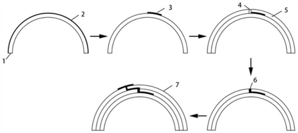
Image

Examples
Embodiment 1
[0075] Example 1: Preparation method of PEEK-based conformal antenna
[0076] (1) Use Fused Deposition (FDM) equipment to print the PEEK antenna support structure base. The raw material of PEEK is wire with a diameter of 1.75mm, the printing temperature is 380-430℃, the printing line speed is 80-120mm / s, and the support structure base needs 100%. filling. The support structure matrix has a tensile strength of 95MPa or more, a flexural strength of 140MPa or more, a tensile modulus of 4GPa, and a flexural modulus of 3.7GPa. The thickness of the support structure base is 3mm, and the projected area diameter of the electronic component is more than 200mm.
[0077] (2) Prepare a feed hole with a diameter of 300μm on the PEEK support structure matrix by laser drilling, use a scanner to reduce the surface roughness of the dielectric layer to Sa=3.2μm, and use a microetching solution to integrate the dielectric structure deal with. The composition of the micro-etching solution is: water...
Embodiment 2
[0085] Embodiment 2: Preparation method of aluminum alloy cold plate base antenna
[0086] (1) Using laser selective melting (SLM) method to prepare curved cold plates according to the design, aluminum alloy material 2A21, cold plate inner runner diameter 3mm, plate thickness 5mm.
[0087] (2) Use a micropen system to prepare an insulating medium layer on the surface of the cold plate. The material is a thermosetting polyimide solution. The polyimide solution is irradiated with an infrared lamp and cured under a temperature gradient below 180°C.
[0088] (3) Microetch the surface of the polyimide dielectric layer, and then prepare a solid film containing palladium ions on the surface.
[0089] (4) A 1064nm nanosecond laser is used to scan according to a preset path. The laser parameters are pulse width 10ns, repetition frequency 50KHz, scanning speed 1500-2000mm / s, laser peak power 30w, and palladium-containing ions are selectively activated on the surface of the curved polyimide laye...
PUM
| Property | Measurement | Unit |
|---|---|---|
| Diameter | aaaaa | aaaaa |
| Tensile strength | aaaaa | aaaaa |
| Bending strength | aaaaa | aaaaa |
Abstract
Description
Claims
Application Information