Preparation method of device based on two-dimensional material

A technology for two-dimensional materials and devices, applied in the field of two-dimensional materials, can solve problems such as restricting the practical process of two-dimensional material devices, reducing the performance of two-dimensional material devices, and contamination of two-dimensional materials, so as to avoid electron beam lithography equipment or Micro transfer system, simple and efficient preparation, performance-enhancing effect

Inactive Publication Date: 2020-09-18
FUDAN UNIV
View PDF7 Cites 0 Cited by
  • Summary
  • Abstract
  • Description
  • Claims
  • Application Information

AI Technical Summary

Problems solved by technology

Their disadvantage is that these two devices are expensive and the operation process is complicated.
In addition, during the preparation of two-dimensional material devices using electron beam lithography or transfer experimental platforms, the surface of two-dimensional materials will be exposed to various chemical substances (including but not limited to polymer resists and solvents), and these residues The substance cannot be completely removed by experimental methods, resulting in contamination of the two-dimensional material, reducing the performance of the prepared two-dimensional material device, and restricting the practical progress of the two-dimensional material device

Method used


Image

  • Preparation method of device based on two-dimensional material
  • Preparation method of device based on two-dimensional material
  • Preparation method of device based on two-dimensional material

Examples


Embodiment 1

[0026] Embodiment 1, a kind of preparation method of the device based on multilayer molybdenum disulfide, comprises the steps:

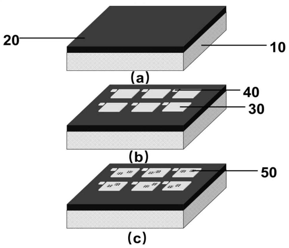
[0027] Step 1: Clean the silicon-based substrate with an oxide layer ultrasonically for 5-10 minutes with acetone and isopropanol, then rinse with deionized water and blow dry with nitrogen. like figure 2 As shown in (a), 10 is a silicon-based substrate, and 20 is an oxide layer. In other embodiments, the target substrate can also be a substrate material or a flexible substrate used in other semiconductor processes;

[0028] Step 2: On the surface of the silicon-based substrate with the oxide layer grown in step 1, use a positive photolithography process to level the glue, use a marking plate containing a labyrinth source-drain electrode pattern to photolithography and pattern development;

[0029] Step 3: Place the developed target substrate in step 2 in the electron beam evaporation system, control the process conditions related to the electron ...

Embodiment 2

[0031] Embodiment 2, a kind of preparation method based on the device of single-layer or few-layer molybdenum disulfide, comprises the steps:

[0032] Step 1-2 is with embodiment 1;

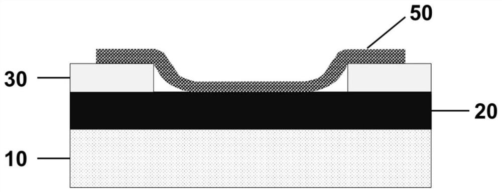
[0033] Step 3: Place the developed target substrate in step 2 in a plasma etching system, control the process parameters of the plasma etching process, and determine the corresponding etching depth according to the thickness of the source and drain electrodes to be grown. Because of the existence of the photoresist, during the etching process, the marks and the source and drain electrodes of the target substrate are etched, while the regions other than the marks and the source and drain electrodes remain intact. The power of plasma etching can be controlled at 300-600 W, and the plasma etching time can be controlled at 10-120 s;

[0034] Step 4: Place the etched target substrate in step 3 in the electron beam evaporation system, control the process conditions related to the electron beam evapora...


PUM

PropertyMeasurementUnit
etching poweraaaaaaaaaa
thicknessaaaaaaaaaa

Abstract

The invention belongs to the technical field of two-dimensional materials, and particularly relates to a preparation method of a device based on a two-dimensional material. According to the invention,the method comprises the steps: employing a mark plate containing a labyrinth type source-drain electrode pattern for forming a mark and a labyrinth type source-drain electrode on a target substratein one step, and then transferring the two-dimensional material to the target substrate, so a device based on the two-dimensional material can be prepared simply and efficiently, and the method is suitable for preparing devices of any substrate; the device comprises a field effect transistor, a resistor, a capacitor and the like.

Description

technical field [0001] The invention belongs to the technical field of two-dimensional materials, and in particular relates to a method for preparing a device based on two-dimensional materials. Background technique [0002] Due to their unique electrical, optical, mechanical, chemical and thermal properties, two-dimensional materials play an increasingly important role in the construction of functional components such as high-performance electronic devices, optoelectronic devices, spintronic devices, energy conversion and memory. important role. For example, molybdenum disulfide has a band gap related to the number of layers (1.2-1.8 eV), high electron mobility (>200cm 2 / Vs), high current switching ratio (>10 8 ), good thermal stability and mechanical properties, and has broad application prospects in many fields such as electrochemical energy storage and conversion, integrated circuits, etc. [0003] At present, the existing preparation schemes of two-dimensional...

Claims


Application Information

Patent Timeline
Patent Type & Authority Applications(China)
IPC IPC(8): H01L21/34H01L21/44H01L29/24H01L29/417H01L29/772H01L23/544H01L49/02
CPCH01L29/66969H01L21/44H01L29/772H01L29/41725H01L23/544H01L29/24H01L28/20H01L28/40H01L28/60
Inventor 杨慧崔四维张一飞方晓生吴东平
Owner FUDAN UNIV
Why Eureka
Try Eureka