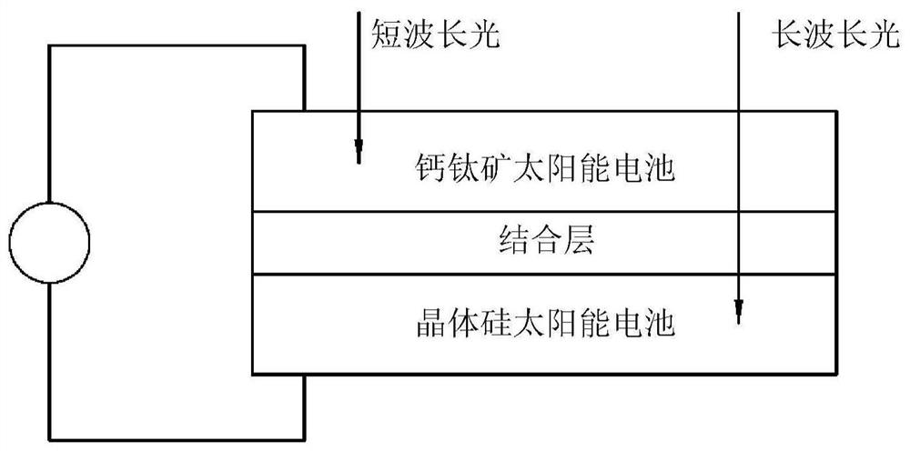
Tandem solar cell manufacturing method
A technology for solar cells and substrates, which can be used in final product manufacturing, sustainable manufacturing/processing, semiconductor/solid-state device manufacturing, etc. It can solve the problems of reducing the fill factor characteristics, and it is difficult to form a unit layer in perovskite solar cells, and achieve excellent Fill factor properties and efficiency, effect of excellent surface roughness properties
- Summary
- Abstract
- Description
- Claims
- Application Information
AI Technical Summary
Problems solved by technology
Method used
Image

Examples
Embodiment 1
[0095] In contrast to Comparative Example 3 above, in Example 1 of the present disclosure, isotropic etching using an aqueous alkaline acid solution in the above SDE method was performed, and then anisotropic etching using an aqueous alkaline solution was performed.
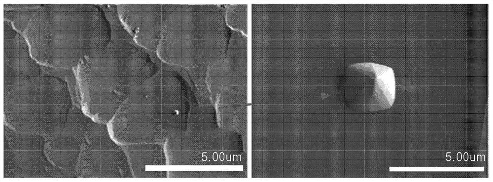
[0096] Figure 9 A picture showing the microstructure in Example 1, in which the bare wafer was pre-cleaned for 10 minutes at room temperature with nitric acid (HNO 3 ) to hydrofluoric acid (HF) ratio isotropically etched for 10 minutes and anisotropically etched for 5 minutes in 5% by weight aqueous sodium hydroxide (NaOH) solution.
[0097] like Figure 9 As shown, the step portion caused by saw marks on the bare wafer was not significantly reduced by isotropic etching, but no sharp cross-sections or surfaces were observed because isotropic etching was performed in all directions, unlike the wafer surface The crystal orientation on the surface is independent to have a surface rounding effect.
[0098] Subseq...
Embodiment 2
[0102] Compared to Example 1 of the present disclosure, an isotropic etch is added in the last step of the SDE of Example 2 of the present disclosure.
[0103] like Figure 10 As shown, in Example 1, saw marks were removed from the surface of the crystalline silicon substrate subjected to isotropic etching and anisotropic etching, and no pyramidal defects existed.
[0104] In Example 2 after continuing the isotropic etching for 10 minutes thereafter, it can be seen that the final substrate has a surface rounded shape by the final isotropic etching, thereby improving the surface roughness and smoothing the curve.
[0105] Figure 11 The mechanism estimated by the present inventors to form the surface of the crystalline silicon substrate by etching in Examples and Comparative Examples of the present disclosure is shown.
[0106] like Figure 11 As shown, a bare silicon substrate cut by a wire saw has saw marks on the surface of the substrate. If anisotropic etching is perfor...
PUM
| Property | Measurement | Unit |
|---|---|---|
| purity | aaaaa | aaaaa |
Abstract
Description
Claims
Application Information
 - R&D
- Intellectual Property
- Life Sciences
- Materials
- Tech Scout
- Unparalleled Data Quality
- Higher Quality Content
- 60% Fewer Hallucinations
Browse by: Latest US Patents, China's latest patents, Technical Efficacy Thesaurus, Application Domain, Technology Topic, Popular Technical Reports.
© 2025 PatSnap. All rights reserved.Legal|Privacy policy|Modern Slavery Act Transparency Statement|Sitemap|About US| Contact US: help@patsnap.com