High-stability phase change memory cell and preparation method thereof
A phase-change storage and phase-change material technology, applied in the field of high-stability phase-change memory cells and their preparation, can solve problems such as inability to achieve three-dimensional confinement, improve device stability, inhibit diffusion and volatilization, and improve thermal stability Effect
- Summary
- Abstract
- Description
- Claims
- Application Information
AI Technical Summary
Problems solved by technology
Method used
Image
Examples
Embodiment 1
[0030] like Figure 1 to Figure 6 As shown, the highly stable phase-change memory cell of the present invention at least includes: a semiconductor substrate, a lower electrode layer, a dielectric isolation layer, a transition layer, a phase-change material region, and an upper electrode, wherein the phase-change material is Phase change materials with three-dimensional confinement capabilities. The phase change material is Ta-Sb-Te, In-Sb-Te, In-Ge-Sb-Te, In-Sc-Sb-Te, Al-Ge-Sb-Te, Ga-Ge-Sb-Te, One of C-Ge-Sb-Te, Hf-Sb-Te, Ta-Sc-Sb-Te, the thickness is 20-100nm, the transition layer is located between the dielectric isolation layer and the phase change material, the transition layer material For WN, TaN, C and other materials, the thickness is 2-10nm.
Embodiment 2
[0032] In this embodiment, Si is prepared by magnetron sputtering 3 N 4 Dielectric material wrapped C-Ge 2 Sb 2 Te 5 Phase change material unit.
[0033] Specific steps:
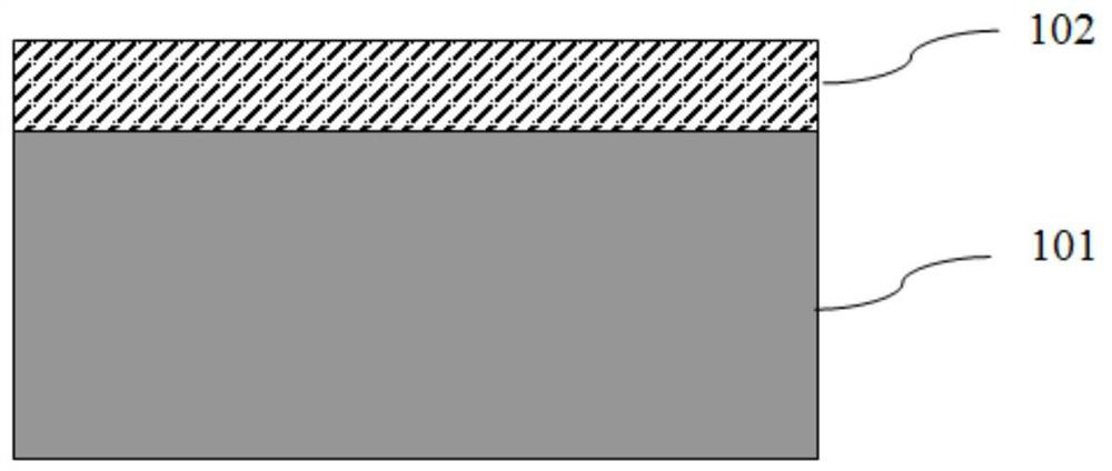
[0034] 1) Clean a (100) oriented semiconductor substrate (such as a silicon substrate), prepare a 100nm thick tungsten electrode 102 (i.e. lower electrode) on a silicon substrate 101, as figure 1 shown.
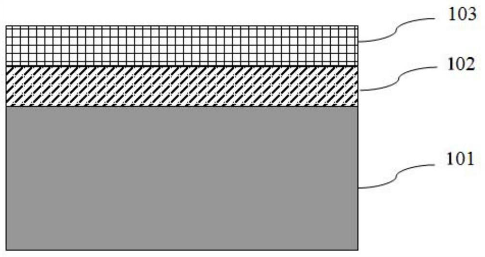
[0035] 2) Deposit a silicon nitride layer 103 (i.e. dielectric isolation layer) on the substrate deposited with tungsten electrodes, with a thickness of 100nm, such as figure 2 shown.
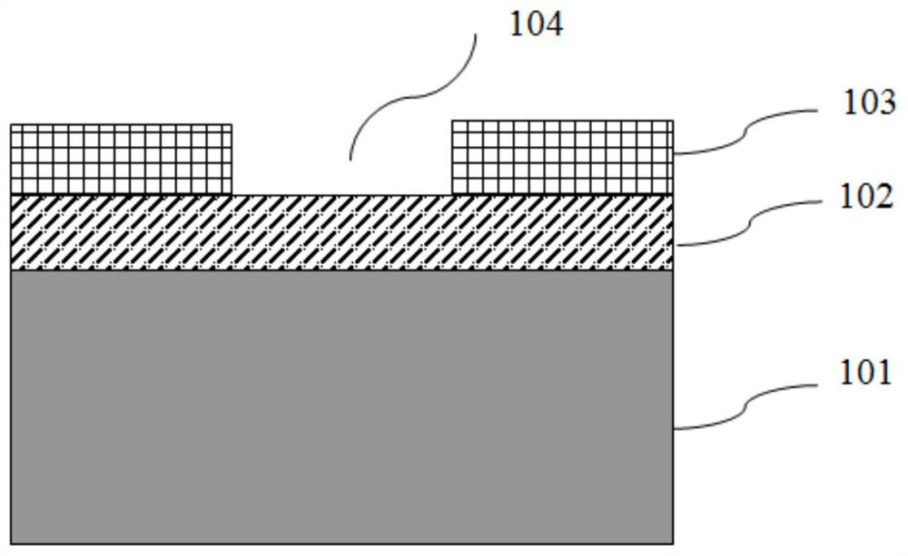
[0036] 3) Carve out a region with a diameter of 200nm on the silicon nitride layer 103 (by an exposure-etching process) as the region 104 where a phase-change material layer needs to be formed. The exposure method used is electron beam exposure, and the etching method is reactive ion etching, such as image 3 shown.
[0037] 4) Prepare a layer of C transition layer on the silicon substrate 1 where a phase change ...
PUM
| Property | Measurement | Unit |
|---|---|---|
| thickness | aaaaa | aaaaa |
| thickness | aaaaa | aaaaa |
| thickness | aaaaa | aaaaa |
Abstract
Description
Claims
Application Information


