Ternary fullerene organic solar cell
A technology of solar cells and fullerenes, applied in circuits, photovoltaic power generation, electrical components, etc., can solve the problems of poor light absorption capacity of fullerene acceptor materials and poor battery stability, and achieves inhibition of bimolecular charge recombination and low cost. , the effect of reducing grain boundary defects
- Summary
- Abstract
- Description
- Claims
- Application Information
AI Technical Summary
Problems solved by technology
Method used
Image
Examples
Embodiment 1
[0033] PTB7-Th:TiC8:PC 71 Preparation of BM (mass ratio = 0.7:0.3:1.5) ternary fullerene organic solar cells.
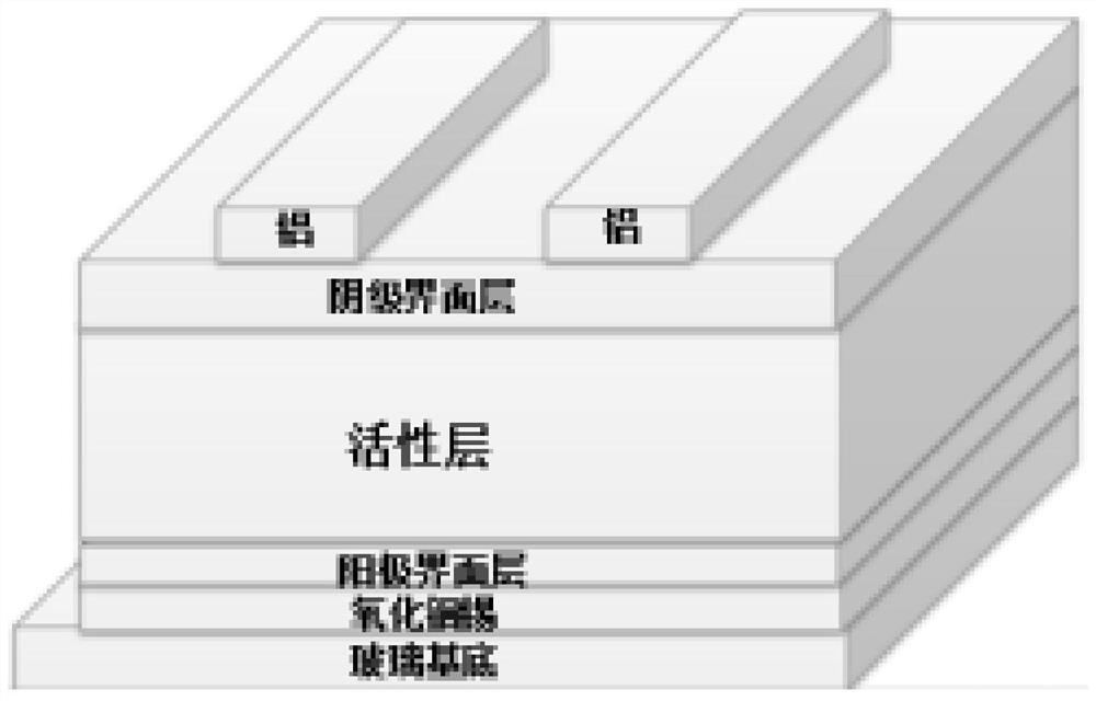
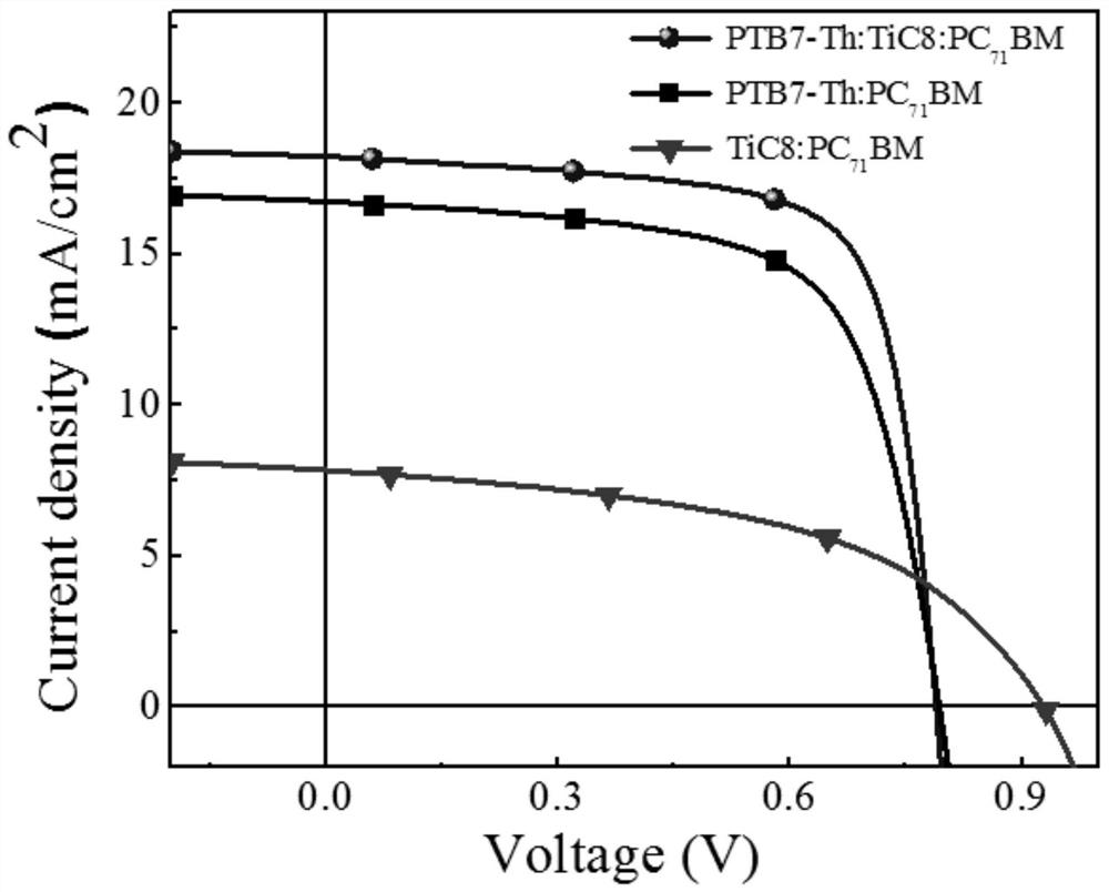
[0034] Treat the clean and transparent conductive anode ITO with ultraviolet ozone for 15 minutes. Prepare PEDOT:PSS (4800rpm, 40s, 30nm) anode buffer layer by spin-coating on its surface, and perform thermal annealing treatment (150°C, 15min); then spin-coat on the anode buffer layer to prepare PTB7-Th:TiC8:PC 71 BM photoactive layer (2000rpm, 60s, 95nm), the mass ratio is 0.7:0.3:1.5; then metal Ca (20nm) and Al (100nm) are sequentially evaporated on the photoactive layer, and the device area is 0.16cm2. Under standard test conditions (AM 1.5, 100mW / cm 2 ), the measured V of the device oc =0.782V,J sc =15.63mA / cm 2 , FF=74.8%, PCE=9.14%.
Embodiment 2
[0036] PTB7-Th:TiC8:PC 71 Preparation of BM (mass ratio = 0.8:0.2:1.5) ternary fullerene organic solar cells.
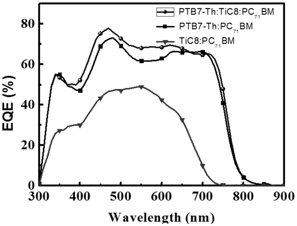
[0037] Treat the clean and transparent conductive anode ITO with ultraviolet ozone for 15 minutes. Prepare PEDOT:PSS (4800rpm, 30s, 30nm) anode buffer layer by spin coating on its surface, and perform thermal annealing treatment (150°C, 15min); then spin coat PTB7-Th:TiC8:PC on the anode buffer layer 71 BM photoactive layer (2000rpm, 60s, 95nm), the mass ratio is 0.8:0.2:1.5; then metal Ca (20nm) and Al (100nm) are sequentially evaporated on the photoactive layer, and the device area is 0.16cm2. Under standard test conditions (AM1.5, 100mW / cm 2 ), the measured open circuit voltage V of the device oc =0.789V,J sc =18.2mA / cm 2 , FF=72.4%, PCE=10.40%.
[0038] When the device area is 0.06cm2, under standard test conditions (AM 1.5, 100mW / cm 2 ), the measured open circuit voltage V of the device oc =0.789V,J sc =19.4mA / cm 2, FF=72.1%, PCE=11.12%.
Embodiment 3
[0040] PTB7-Th:TiC8:PC 71 Preparation of BM (mass ratio = 0.9:0.1:1.5) ternary fullerene organic solar cells.
[0041] Treat the clean and transparent conductive anode ITO with ultraviolet ozone for 15 minutes. Prepare PEDOT:PSS (4800rpm, 40s, 30nm) anode buffer layer by spin-coating on its surface, and perform thermal annealing treatment (150°C, 15min); then spin-coat on the anode buffer layer to prepare PTB7-Th:TiC8:PC 71 BM photoactive layer (2000rpm, 60s, 95nm), mass ratio 0.9:0.1:1.5; then sequentially evaporate metal Ca (20nm) and Al (100nm) on the photoactive layer, device area 0.16cm2. Under standard test conditions (AM1.5, 100mW / cm 2 ), the measured V of the device oc =0.785V,J sc =17.41mA / cm 2 , FF=72.3%, PCE=9.88%.
PUM
| Property | Measurement | Unit |
|---|---|---|
| Thickness | aaaaa | aaaaa |
| Short circuit current | aaaaa | aaaaa |
| Open circuit voltage | aaaaa | aaaaa |
Abstract
Description
Claims
Application Information


