A kind of pyridoimidazopyrrole compound and its application
A technology of pyridimidazole and compounds, which is applied in the field of organic electroluminescent functional materials, can solve the problems of TADF host materials without performance, and achieve the effects of improved lifespan, high carrier transport performance, and good film-forming performance
- Summary
- Abstract
- Description
- Claims
- Application Information
AI Technical Summary
Problems solved by technology
Method used
Image
Examples
preparation example Construction
[0028] Below, we provide specific synthetic methods for preparing some of the above-mentioned compounds and some intermediates selected for the preparation of the compounds. The synthetic steps are as follows:
[0029] The specific synthesis process of the compound intermediate of general structural formula (I) is as follows:
[0030]
[0031] Compound 1-1 was added to a mixed solution of concentrated sulfuric acid and concentrated nitric acid, heated to 100°C for 2 hours, and the reaction solution was slowly poured into ice water under stirring conditions, the solid was precipitated by stirring, and filtered. The filter cake was washed with water until neutral, dried, and purified by silica gel column to obtain compound 1-2.
[0032]
[0033] Add toluene in the three-necked flask, then add 1mol of compound 1-2, 1.1mol of compound 1-3, 0.05mol of 2-dicyclohexylphosphine-2,4,6-triisopropylbiphenyl, 2.2mol 0.025 mol of tris(dibenzylideneacetone) dipalladium was added unde...
Embodiment 1
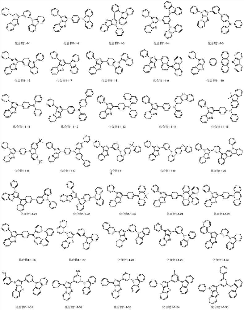
[0107] Transparent substrate layer 1 / ITO anode layer 2 / hole transport layer 3 (TAPC, thickness is 40nm) / luminescent layer 4 (including host material CBP, sensitizing material compound 1-1-35, doping material TCzCN, according to 93: 5:2 mass ratio mixing, thickness 30nm) / electron transport layer 5 (TPBi, thickness 40nm) / electron injection layer 6 (LiF, thickness 1nm) / cathode reflective electrode layer Al.
[0108] The structure of some materials used in the device is as follows:
[0109]
[0110] Concrete preparation process is as follows:
[0111] The transparent substrate layer is a transparent substrate, such as transparent PI film, glass and the like.
[0112] The ITO anode layer is washed, followed by alkali washing, ultrapure water washing, drying, and then ultraviolet-ozone washing to remove organic residues on the transparent ITO surface.
[0113] On the above-mentioned ITO anode layer, TAPC with a film thickness of 40 nm was deposited as the hole transport layer 1...
Embodiment 2
[0120] Same as Example 1, except that: the light-emitting layer 4 includes host material CBP, sensitizing material compound 2-2-17, and dopant material TCzCN, with a mass ratio of 93:5:2 and a thickness of 30 nm.
PUM
| Property | Measurement | Unit |
|---|---|---|
| thickness | aaaaa | aaaaa |
| thickness | aaaaa | aaaaa |
| thickness | aaaaa | aaaaa |
Abstract
Description
Claims
Application Information


